HI3-0303-5 データシートの表示(PDF) - Intersil
部品番号
コンポーネント説明
メーカー
HI3-0303-5 Datasheet PDF : 11 Pages
| |||
HI-303
Absolute Maximum Ratings
Voltage Between Supplies (V+ to V-) . . . . . . . . . . . . . . . . 44V (±22V)
Digital Input Voltage . . . . . . . . . . . . . . . . . . . . . . (V+) +4V to (V-) -4V
Analog Input Voltage . . . . . . . . . . . . . . . . . . (V+) +1.5V to (V-) -1.5V
Typical Derating Factor . . . . . . . . . 1.5mA/MHz Increase in ICCOP
ESD Classification . . . . . . . . . . . . . . . . . . . . . . . . . . . . . . . . . Class 1
Operating Conditions
Temperature Range
HI-303-2 . . . . . . . . . . . . . . . . . . . . . . . . . . . . . . . . -55oC to 125oC
HI-303-5 . . . . . . . . . . . . . . . . . . . . . . . . . . . . . . . . . . 0oC to 75oC
HI-303-9 . . . . . . . . . . . . . . . . . . . . . . . . . . . . . . . . . -40oC to 85oC
Thermal Information
Thermal Resistance (Typical, Note 1)
θJA (oC/W) θJC (oC/W)
CERDIP Package. . . . . . . . . . . . . . . . .
80
24
PDIP Package . . . . . . . . . . . . . . . . . . .
90
N/A
SOIC Package . . . . . . . . . . . . . . . . . . . 120
N/A
Maximum Junction Temperature
Ceramic Packages . . . . . . . . . . . . . . . . . . . . . . . . . . . . . . . 175oC
Plastic Packages . . . . . . . . . . . . . . . . . . . . . . . . . . . . . . . . 150oC
Maximum Storage Temperature Range . . . . . . . . . . -65oC to 150oC
Maximum Lead Temperature (Soldering 10s) . . . . . . . . . . . . 300oC
(SOIC - Lead Tips Only)
CAUTION: Stresses above those listed in “Absolute Maximum Ratings” may cause permanent damage to the device. This is a stress only rating and operation of the
device at these or any other conditions above those indicated in the operational sections of this specification is not implied.
NOTE:
1. θJA is measured with the component mounted on a low effective thermal conductivity test board in free air. See Tech Brief TB379 for details.
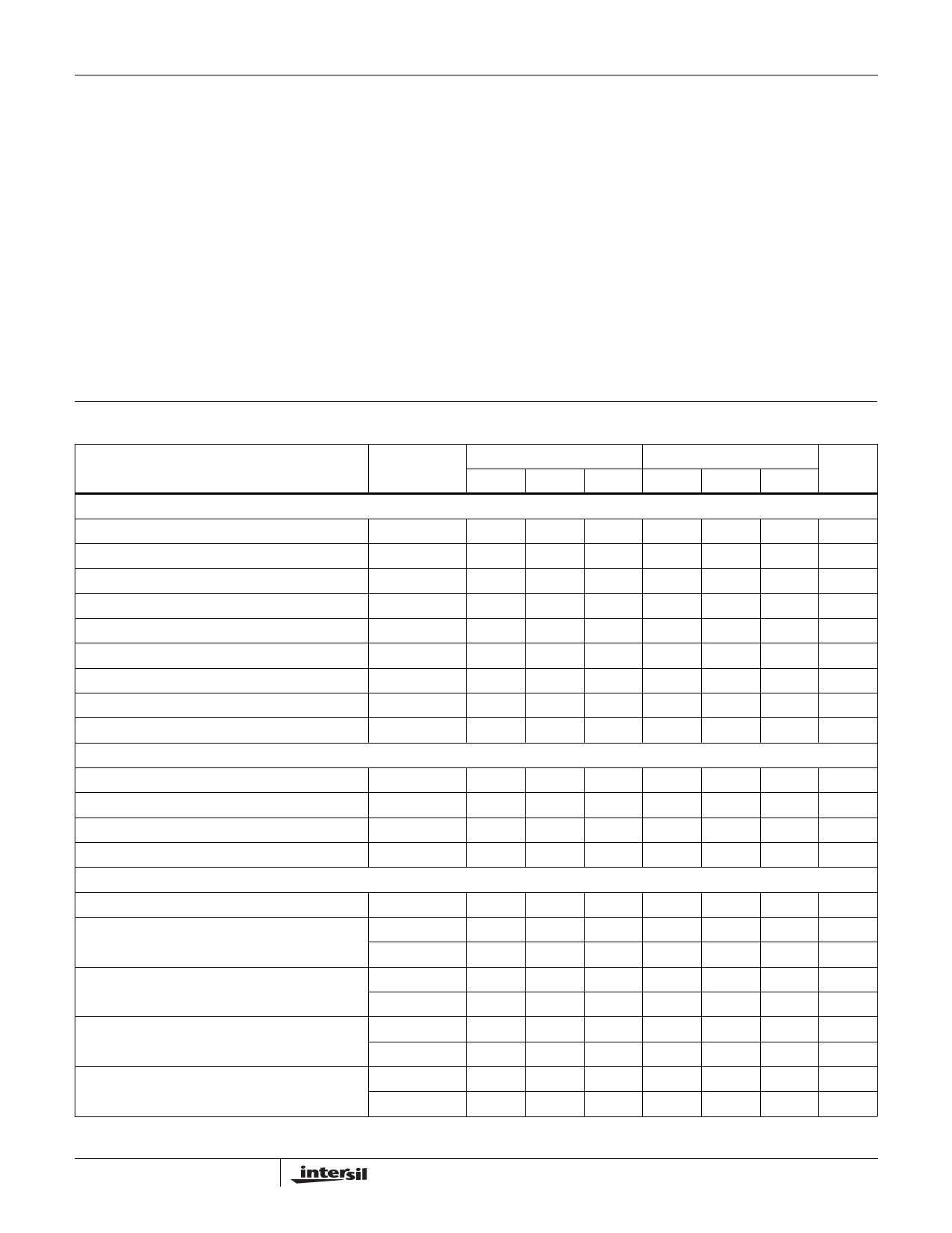
Electrical Specifications Supplies = +15V, -15V; VIN = Logic Input. VIN - for Logic “1” = 4V, for Logic “0” = 0.8V.
Unless Otherwise Specified
PARAMETER
TEMP
(oC)
-2
-5, -9
MIN
TYP
MAX
MIN
TYP
DYNAMIC CHARACTERISTICS
Switch ON Time, tON
Switch OFF Time, tOFF
Break-Before-Make Delay, tOPEN
Charge Injection Voltage, ∆V (Note 7)
25
-
210
300
-
210
25
-
160
250
-
160
25
-
60
-
-
60
25
-
3
-
-
3
OFF Isolation (Note 6)
25
-
60
-
-
60
Input Switch Capacitance, CS(OFF)
Output Switch Capacitance, CD(OFF)
Output Switch Capacitance, CD(ON)
Digital Input Capacitance, CIN
DIGITAL INPUT CHARACTERISTICS
25
-
16
-
-
16
25
-
14
-
-
14
25
-
35
-
-
35
25
-
5
-
-
5
Input Low Level, VINL
Input High Level, VINH (Note 10)
Input Leakage Current (Low), IINL (Note 5)
Input Leakage Current (High), IINH (Note 5)
ANALOG SWITCH CHARACTERISTICS
Full
-
-
0.8
-
-
Full
4
-
-
4
-
Full
-
-
1
-
-
Full
-
-
1
-
-
Analog Signal Range
Full
-15
-
+15
-15
-
ON Resistance, rON (Note 2)
25
-
35
50
-
35
Full
-
40
75
-
40
OFF Input Leakage Current, IS(OFF) (Note 3)
25
-
0.04
1
-
0.04
Full
-
1
100
-
0.2
OFF Output Leakage Current, ID(OFF) (Note 3)
25
-
0.04
1
-
0.04
Full
-
1
100
-
0.2
ON Leakage Current, ID(ON) (Note 4)
25
-
0.03
1
-
0.03
Full
-
0.5
100
-
0.2
MAX UNITS
300
ns
250
ns
-
ns
-
mV
-
dB
-
pF
-
pF
-
pF
-
pF
0.8
V
-
V
1
µA
1
µA
+15
V
50
Ω
75
Ω
5
nA
100
nA
5
nA
100
nA
5
nA
100
nA
3
FN3125.10
November 17, 2004
Share Link: 