HI7191(1998) データシートの表示(PDF) - Intersil
部品番号
コンポーネント説明
メーカー
HI7191 Datasheet PDF : 24 Pages
| |||
HI7191
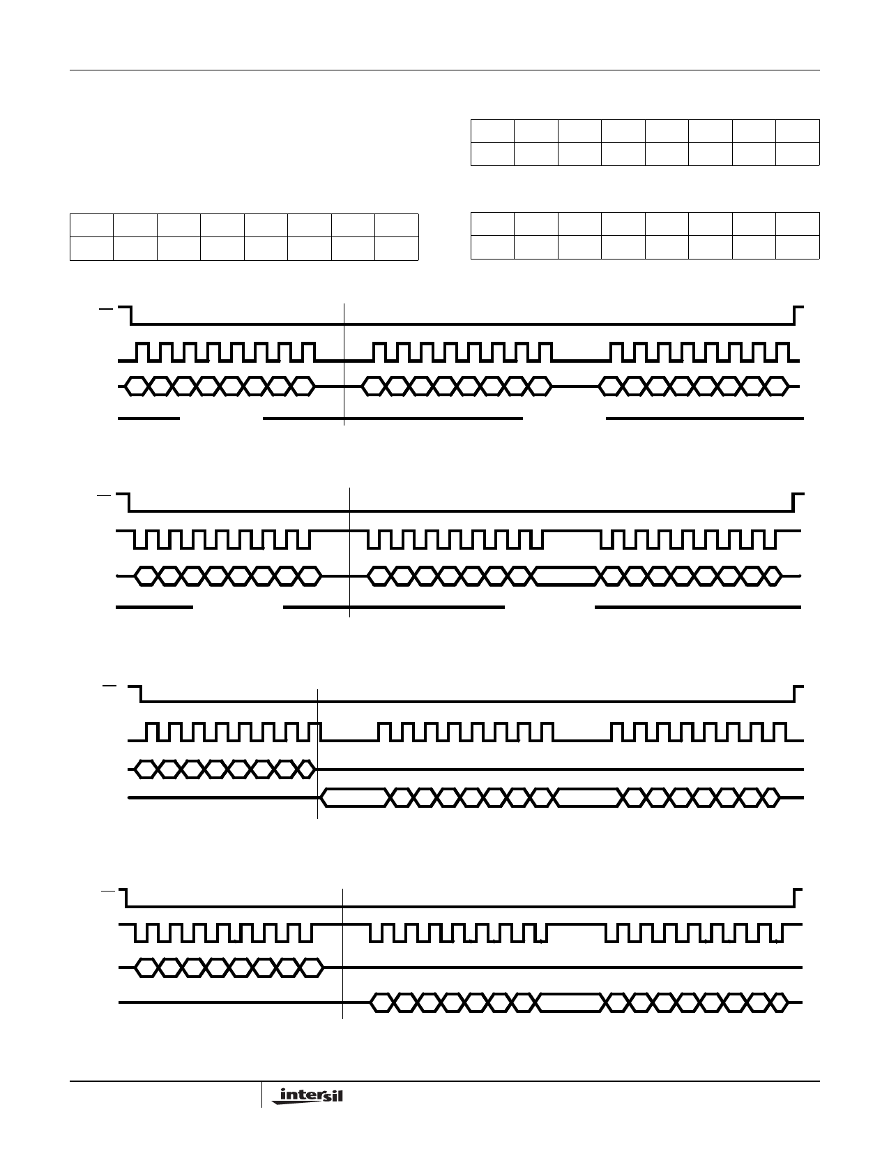
IR WRITE PHASE
CS
DATA TRANSFER PHASE - TWO-BYTE READ
SCLK
SDIO
SDO
I0 I1 I2 I3 I4 I5 I6 I7
B15
B0 B1 B2 B3 B4 B5 B6
B7
B8 B9 B10 B11 B12 B13 B14
THREE-STATE
THREE-STATE
FIGURE 19. DATA READ CYCLE, 2-WIRE CONFIGURATION, SCLK IDLE HIGH
Control Register
The Control Register contains 24-bits to control the various
sections of the HI7191. This register is a read/write
register.
BYTE 2
MSB 22
21
20
19
18
17
16
DC FP10 FP9 FP8 FP7 FP6 FP5 FP4
BYTE 1
15
14
13
12
11
10
9
8
FP3 FP2 FP1 FP0 MD2 MD1 MD0 B/U
BYTE 0
7
6
5
4
3
2
1 LSB
G2 G1 G0 BO SB BD MSB SDL
DC - Bit 23 is the Data Coding Bit used to select between
two’s complementary and offset binary data coding. When
this bit is set (DC = 1) the data in the Data Output Register
will be two’s complement. When cleared (DC = 0) this data
will be offset binary. When operating in the unipolar mode
the output data is available in straight binary only (the DC bit
is ignored). This bit is cleared after a RESET is applied to
the part.
FP10 through FP0 - Bits 22 through 12 are the Filter pro-
gramming bits that determine the frequency response of the
digital filter. These bits determine the filter cutoff frequency,
the position of the first notch and the data rate of the HI7191.
The first notch of the filter is equal to the decimation rate and
can be determined by the formula:
fNOTCH = fOSC /(512 x CODE)
where CODE is the decimal equivalent of the value in FP10
through FP0. The values that can be programmed into these
bits are 10 to 2047 decimal, which allows a conversion rate
range of 9.54Hz to 1.953kHz when using a 10MHz clock.
Changing the filter notch frequency, as well as the selected
gain, impacts resolution. The output data rate (or effective
conversion time) for the device is equal to the frequency
selected for the first notch to the filter. For example, if the first
notch of the filter is selected at 50Hz then a new word is avail-
able at a 50Hz rate or every 20ms. If the first notch is at 1kHz
a new word is available every 1ms.
The settling-time of the converter to a full scale step input
change is between 3 and 4 times the data rate. For example,
with the first filter notch at 50Hz, the worst case settling time to
a full scale step input change is 80ms. If the first notch is 1kHz,
the settling time to a full scale input step is 4ms maximum.
The -3dB frequency is determined by the programmed first
notch frequency according to the relationship:
f -3dB = 0.262 x fNOTCH.
MD2 through MD0 - Bits 11 through 9 are the Operational
Modes of the converter. See Table 4 for the Operational
Modes description. After a RESET is applied to the part these
bits are set to the self calibration mode.
B/U - Bit 8 is the Bipolar/Unipolar select bit. When this bit is
set the HI7191 is configured for bipolar operation. When this
bit is reset the part is in unipolar mode. This bit is set after a
RESET is applied to the part.
G2 through G0 - Bits 7 through 5 select the gain of the input
analog signal. The gain is accomplished through a program-
mable gain instrumentation amplifier that gains up incoming
signals from 1 to 8. This is achieved by using a switched
capacitor voltage multiplier network preceding the modulator.
The higher gains (i.e., 16 to 128) are achieved through a com-
bination of a PGIA gain of 8 and a digital multiply after the dig-
ital filter (see Table 7). The gain will affect noise and Signal to
Noise Ratio of the conversion. These bits are cleared to a gain
of 1 (G2, G1, G0 = 000) after a RESET is applied to the part.
TABLE 7. GAIN SELECT BITS
G2 G1 G0 GAIN
GAIN ACHIEVED
0
0
0
1 PGIA = 1, Filter Multiply = 1
0
0
1
2 PGIA = 2, Filter Multiply = 1
0
1
0
4 PGIA = 4, Filter Multiply = 1
0
1
1
8 PGIA = 8, Filter Multiply = 1
1
0
0
16 PGIA = 8, Filter Multiply = 2
1
0
1
32 PGIA = 8, Filter Multiply = 4
1
1
0
64 PGIA = 8, Filter Multiply = 8
1
1
1
128 PGIA = 8, Filter Multiply = 16
1915
Share Link: 