HI7191(1998) データシートの表示(PDF) - Intersil
部品番号
コンポーネント説明
メーカー
HI7191 Datasheet PDF : 24 Pages
| |||
HI7191
BO - Bit 4 is the Transducer Burn-Out Current source enable
bit. When this bit is set (BO = 1) the burn-out current source
connected to VINHI internally is enabled. This current source
can be used to detect the presence of an external connection
to VINHI. This bit is cleared after a RESET is applied to the
part.
SB - Bit 3 is the Standby Mode enable bit used to put the
HI7191 in a lower power/standby mode. When this bit is set
(SB = 1) the filter nodes are halted, the DRDY line is set high
and the modulator clock is disabled. When this bit is cleared
the HI7191 begins operation as described by the contents of
the Control Register. For example, if the Control Register is
programmed for Self Calibration Mode and a notch frequency
to 10Hz, the HI7191 will perform the self calibration before
providing the data at the 10Hz rate. This bit is cleared after a
RESET is applied to the part.
BD - Bit 2 is the Byte Direction bit used to select the multi-byte
access ordering. The bit determines the either ascending or
descending order access for the multi-byte registers. When
set (BD = 1) the user can access multi-byte registers in
ascending byte order and when cleared (BD = 0) the multi-
byte registers are accessed in descending byte order. This bit
is cleared after a RESET is applied to the part.
MSB - Bit 1 is used to select whether a serial data transfer is
MSB or LSB first. This bit allows the user to change the order
that data can be transmitted or received by the HI7191. When
this bit is cleared (MSB = 0) the MSB is the first bit in a serial
data transfer. If set (MSB = 1), the LSB is the first bit trans-
ferred in the serial data stream. This bit is cleared after a
RESET is applied to the part.
SDL - Bit 0 is the Serial Data Line control bit. This bit selects
the transfer protocol of the serial interface. When this bit is
cleared (SDL = 0), both read and write data transfers are done
using the SDIO line. When set (SDL = 1), write transfers are
done on the SDIO line and read transfers are done on the SDO
line. This bit is cleared after a RESET is applied to the part.
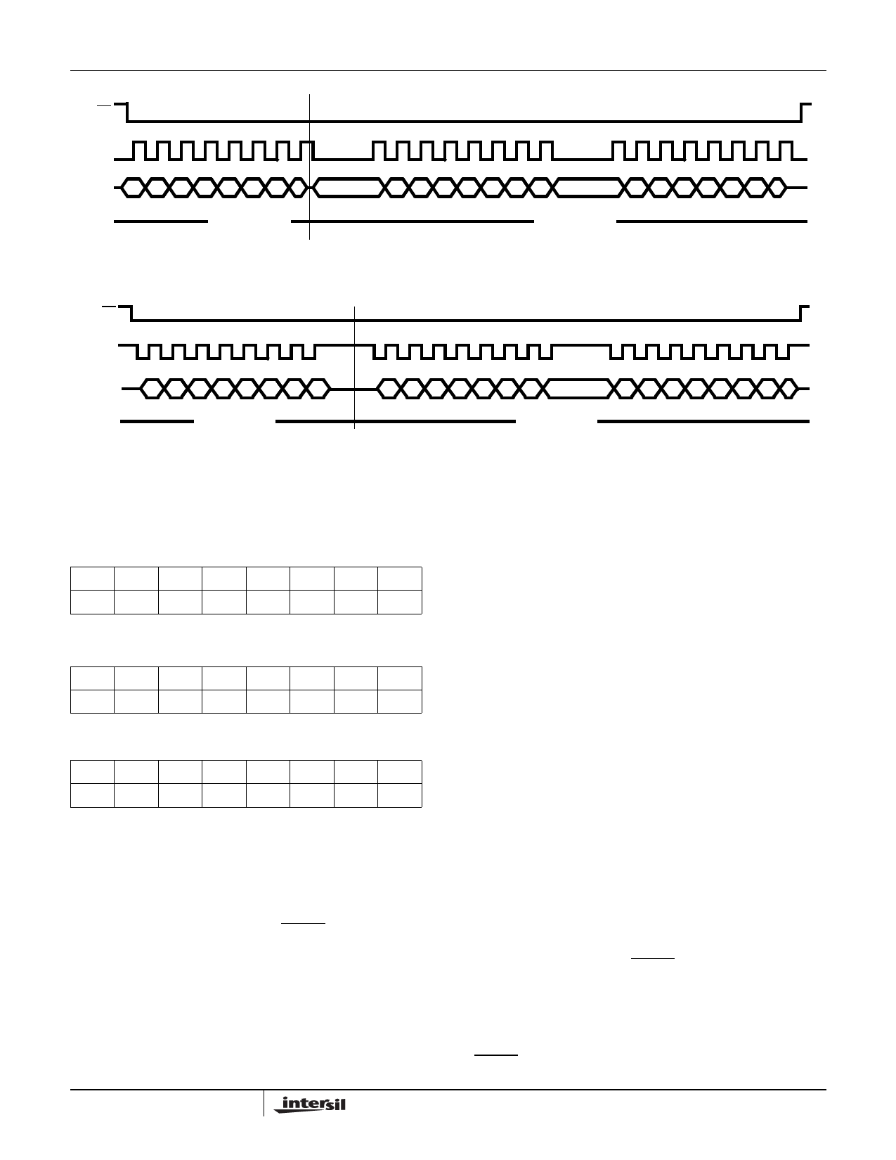
Reading the Data Output Register
The HI7191 generates an active low interrupt (DRDY) indicat-
ing valid conversion results are available for reading. At this
time the Data Output Register contains the latest conversion
result available from the HI7191. Data integrity is maintained
at the serial output port but it is possible to miss a conversion
result if the Data Output Register is not read within a given
period of time. Maintaining data integrity means that if a Data
Output Register read of conversion N is begun but not fin-
ished before the next conversion (conversion N + 1) is com-
plete, the DRDY line remains active low and the data being
read is not overwritten.
In addition to the Data Output Register, the HI7191 has a one
conversion result storage buffer. No conversion results will be
lost if the following constraints are met.
1) A Data Output Register read cycle is started for a given
conversion (conversion X) 1/fN - (128*1/fOSC) after DRDY ini-
tially goes active low. Failure to start the read cycle may result
in conversion X + 1 data overwriting conversion X results. For
example, with fOSC
start within 1/2000 -
1=2180(1M/1H0z6,)fN=
= 2kHz, the read cycle must
487µs after DRDY went low.
2) The Data Output Register read cycle for conversion X must
be completed within 2(1/fN)-1440(1/fOSC) after DRDY initially
goes active low. If the read cycle for conversion X is not com-
plete within this time the results of conversion X + 1 are lost
and results from conversion X + 2 are now stored in the data
output word buffer.
Completing the Data Output Register read cycle inactivates
the DRDY interrupt. If the one word data output buffer is full
when this read is complete this data will be immediately trans-
ferred to the Data Output Register and a new DRDY interrupt
will be issued after the minimum DRDY pulse high time is met.
Writing the Control Register
If data is written to byte 2 and/or byte 1 of the Control Register
the DRDY output is taken high and the device re-calibrates if
written to a calibration mode. This action is taken because it is
assumed that by writing byte 2 or byte 1 that the user either
reprogrammed the filter or changed modes of the part. How-
ever, if a single data byte is written to byte 0, it is assumed that
the gain has NOT been changed. It is up to the user to re-cali-
brate the HI7191 after the gain has been changed by this
method. It is recommended that the entire Control Register be
written to when changing the selected gain. This ensures that
the part is re-calibrated before the DRDY signal goes low indi-
cating valid data is available.
Offset Calibration Register
The Offset Calibration Register is a 24-bit register containing
the offset correction factor. This register is indeterminate on
power-up but will contain a Self Calibration correction value
after a RESET has been applied.
BYTE 2
MSB 22
21
20
19
18
17
16
O23 O22 O21 O20 O19 O18 O17 O16
BYTE 1
15
14
13
12
11
10
9
8
O15 O14 O13 O12 O11 O10 O9 O8
BYTE 0
7
6
5
4
3
2
1 LSB
O7 O6 O5 O4 O3 O2 O1 O0
The Offset Calibration Register holds the value that corrects
the filter output data to all 0’s when the analog input is 0V.
1916
Share Link: 