HM62256BLFP-7T гГЗгГЉгВњгВЈгГЉгГИгБЃи°®з§ЇпЉИPDFпЉЙ - Hitachi -> Renesas Electronics
йГ®еУБзХ™еПЈ
гВ≥гГ≥гГЭгГЉгГНгГ≥гГИи™ђжШО
гГ°гГЉгВЂгГЉ
HM62256BLFP-7T Datasheet PDF : 20 Pages
| |||
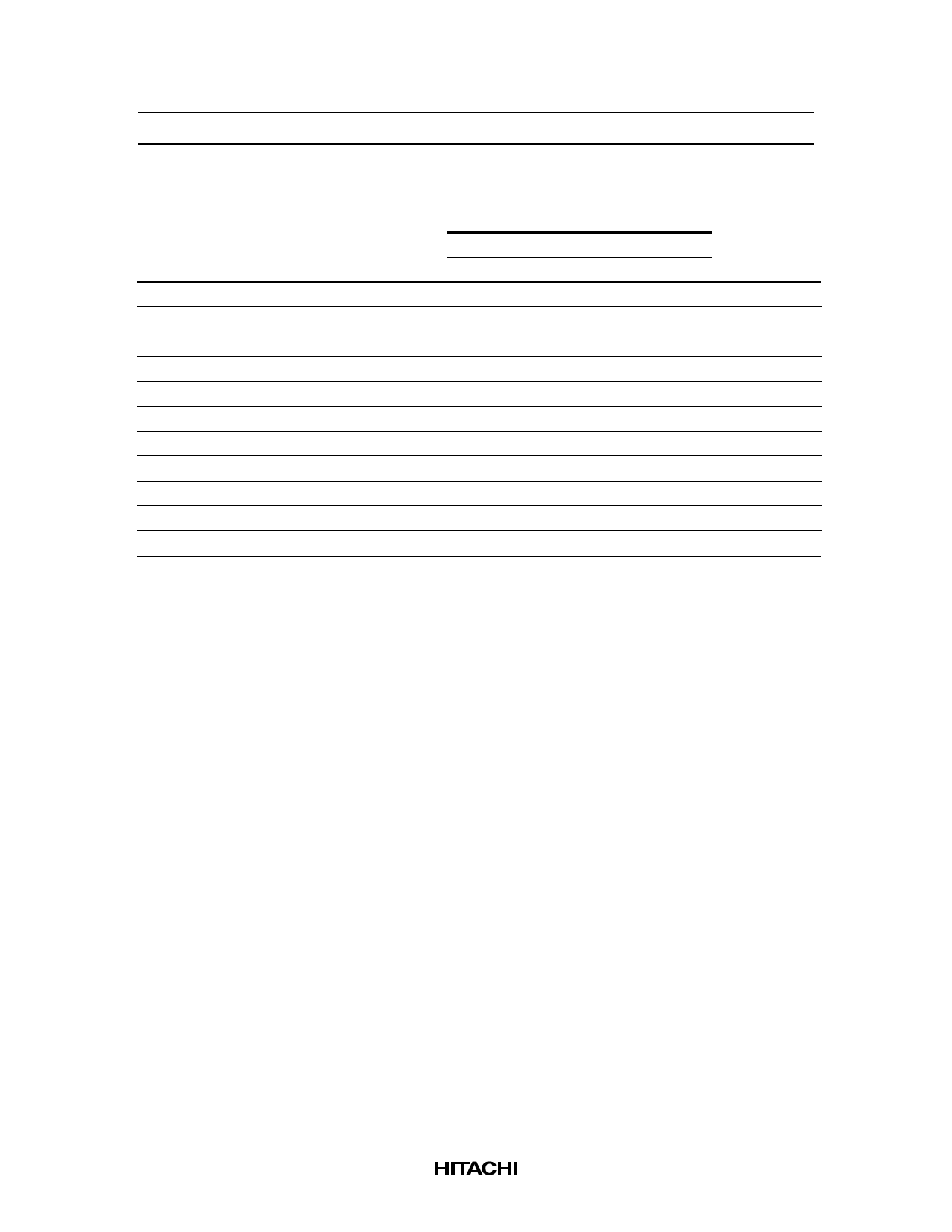
HM62256B Series
Write Cycle
HM62256B
-5
-7
-8
Parameter
Symbol Min Max Min Max Min Max Unit Notes
Write cycle time
t WC
55 вАФ 70 вАФ 85 вАФ ns
Chip selection to end of write
t CW
40 вАФ 60 вАФ 75 вАФ ns
5
Address setup time
t AS
0
вАФ0
вАФ0
вАФ ns
6
Address valid to end of write
t AW
40 вАФ 60 вАФ 75 вАФ ns
Write pulse width
t WP
35 вАФ 50 вАФ 55 вАФ ns
4, 13
Write recovery time
t WR
0
вАФ0
вАФ0
вАФ ns
7
Write to output in high-Z
t WHZ
0
20 0
25 0
30 ns
1, 2, 8
Data to write time overlap
t DW
25 вАФ 30 вАФ 35 вАФ ns
Data hold from write time
t DH
0
вАФ0
вАФ0
вАФ ns
Output active from end of write
t OW
5
вАФ5
вАФ5
вАФ ns
2
Output disable to output in High-Z
t OHZ
0
20 0
25 0
30 ns
1, 2, 8
Notes: 1. tCHZ, tOHZ and tWHZ are defined as the time at which the outputs achieve the open circuit conditions
and are not referred to output voltage levels.
2. This parameter is sampled and not 100% tested.
3. Address must be valid prior to or simultaneously with CS going low.
4. A write occurs during the overlap of a low CS and a low WE. A write begins at the latest
transition of CS going low or WE going low. A write ends at the earliest transition of CS going
high or WE going high. tWP is measured from the beginning of write to the end of write.
5. tCW is measured from CS going low to the end of write.
6. tAS is measured from the address valid to the beginning of write.
7. tWR is measured from the earliest of CS or WE going high to the end of write cycle.
8. During this period, I/O pins are in the output state; therefore, the input signals of the opposite
phase to the outputs must not be applied.
9. If CS goes low simultaneously with WE going low or after WE going low, the outputs remain in
the high impedance state.
10. Dout is the same phase of the latest written data in this write cycle.
11. Dout is the read data of next address.
12. If CS is low during this period, I/O pins are in the output state. Therefore, the input signals of the
opposite phase to the outputs must not be applied to them.
13. In the write cycle with OE low fixed, tWP must satisfy the following equation to avoid a problem of
data bus contention.
tWP вЙ• tDW min + tWHZ max
8
Share Link: 