HM91710A データシートの表示(PDF) - ELAN Microelectronics
部品番号
コンポーネント説明
メーカー
HM91710A Datasheet PDF : 19 Pages
| |||
HM91710A/B
TONE/PULES SWITCHABLE DIALER
PIN DESCRIPTION
Symbol
Function
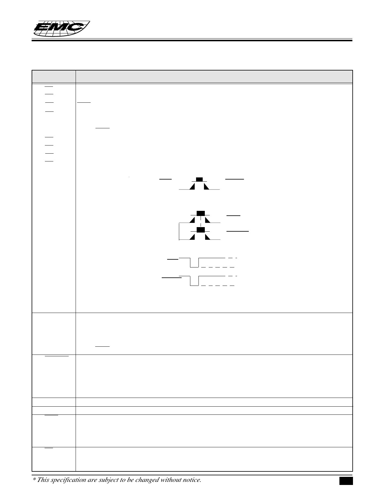
C1
Provides keyboard scanning .
C2
a. Keyboard scanning:
C3
HKS pin is LOW, the column group stays in "HIGH" stays and row group stays in "LOW" state.
C4
The key pad is compatible with the standard dual contact matrix keyboard (as Figure 1b.), the
inexpensive single contact keyboard (as Figure 1a.), and electronic input (as Figure 1c.).
When HKS is "low", a valid key entry is defined by related Row & Column connection or by
R1
electronic input; (as show in Figure 1c).
R2
Activation of two or more keys will result in no response, except for single key.
R3
To avoid keyboard bouncing error, this chip provides built-in debounce circuit. (The debounce
R4
time = 20 ms.)
Row
Column
Figure 1a : Single contact form keyboard configuration
Row
Column
Figure 1b : Dual contact form keyboard configuration
VDD
Row
VSS
VDD
Column
VSS
Figure 1c : Electronic signal input keyboard configuration
OSCI
OSCO
XMUTE
V
SS
VDD
HKS
PO
Oscillator input & Oscillator output pins.
The 3.579545 MHz oscillator is formed by a built-in inverter inside of this chip and by connecting a
3.579545 MHz crystal or a ceramic resonator across the OSCI and OSCO pins. (built-in feedback
resistor and capacitor)
When HKS is low, a valid key-in may turn on this oscillator and generates a 3.579545 MHz clock.
Mute output pins.
NMOS open drain output structure.
The output is in low state during dialing sequence (both Pulse and Tone mode) otherwise this pin is
"high-impedance".
Long (continue) Mute.
Negative power supply pin.
Positive power supply pin.
Hook switch input pin.
When the handset is in ON-HOOK state, this pin must be pulled "high" in order to disable the dialing
operation and decrease the power consumption.
When in OFF-HOOK state, the HKS pin must be pulled "low" state for all function operation.
Pulse output signal pin.
NMOS open drain output structure.
The output is "low" during pulse dialing and Flash operation, otherwise this output is "floating".
* This specification are subject to be changed without notice.
1.7.2002 3
Share Link: 