NVM3060 データシートの表示(PDF) - Micronas
部品番号
コンポーネント説明
メーカー
NVM3060 Datasheet PDF : 13 Pages
| |||
NVM 3060
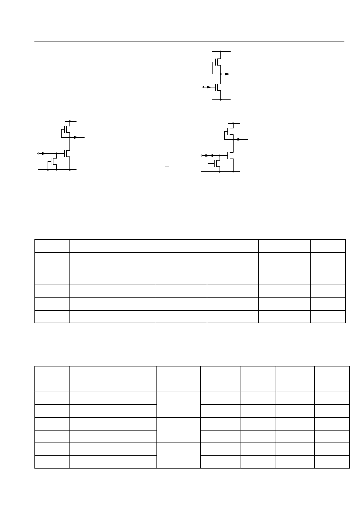
2.4. Pin Circuits
The following figures show schematically the circuitry at
the various pins. The integrated protection structures
are not shown. The letter “E” means enhancement,
the letter “D” depletion.
VSUP
D
E
D
GND
Fig. 2–2:
Pins 2 and 3, Input S
VSUP
D
E
GND
VSUP
D
E
E
GND
Fig. 2–3:
Pins 4, 5, and 6, Inputs
Fig. 2–4:
Pin 7, Input/Output
2.5. Electrical Characteristics
All Voltages are referred to ground.
2.5.1. Absolute Maximum Ratings
Symbol
TA
TS
VSUP
VI
IO
Parameter
Ambient Operating
Temperature
Storage Temperature
Supply Voltage
Input Voltage
Output Current
Pin No.
–
–
8
2 to 7
7
* Stored data may be affected by TS above +85 °C
Min.
0
–40
–0.5
–0.3 V
–
Max.
65
+125*
+6
VSUP
5
2.5.2. Recommended Operating Conditions
Symbol
VSUP
VIL
VIH
VREIL
VREIH
t4
t7
Parameter
Supply Voltage
Input Low Voltage
Input High Voltage
Reset Input Low Voltage
Reset Input High Voltage
VSUP – VREI Delay Time*
VREI – VSUP Delay Time*
*see Fig. 2–5
Pin No.
8
2, 3, 5 to 7
4
4, 8
Min.
4.75
–
2.4
–
2.4
0
0
Typ.
5.0
–
–
–
–
–
–
Max.
5.25
0.8
–
1.3
–
–
–
Unit
°C
°C
V
–
mA
Unit
V
V
V
V
V
ms
ms
5
Share Link: 