HS3140B-4/833 データシートの表示(PDF) - Signal Processing Technologies
部品番号
コンポーネント説明
メーカー
HS3140B-4/833 Datasheet PDF : 8 Pages
| |||
PIN ASSIGNMENTS…
Pin 1 – IO1 – Current Output 1.
Pin 2 – IO2 – Current Output 2.
Pin 3 – GND – Ground.
Pin 4 – DB13 – MSB, Data Bit 1.
Pin 5 – DB12 – Data Bit 2.
Pin 6 – DB11 – Data Bit 3.
Pin 7 – DB10 – Data Bit 4.
Pin 8 – DB9 – Data Bit 5.
Pin 9 – DB8 – Data Bit 6.
Pin 10 – DB7 – Data Bit 7.
Pin 11 – DB6 – Data Bit 8.
Pin 12 – DB5 – Data Bit 9.
Pin 13 – DB4 – Data Bit 10.
Pin 14 – DB3 – Data Bit 11.
Pin 15 – DB2 – Data Bit 12.
Pin 16 – DB1 – Data Bit 13.
Pin 17 – DB0 – LSB, Data Bit 14.
Pin 18 – VDD – Positive Supply Voltage.
Pin 19 – VREF – Reference Voltage Input.
Pin 20 – RFB – Feedback Resistor.
FEATURES…
The SP7514 and HS3140 are precision 14-bit multi-
plying DACs. The DACs are implemented as a one-
chip CMOS circuit with a resistor ladder network.
Three output lines are provided on the DACs to allow
unipolar and bipolar output connection with a mini-
mum of external components. The feedback resistor
is internal. The resistor ladder network termination is
externally available, thus eliminating an external re-
sistor for the 1 LSB offset in bipolar mode.
The SP7514 is available for use in commercial and
industrial temperature ranges, packaged in a 20-pin
SOIC. The HS3140 is available in commercial
and military temperature ranges, packaged in a
20–pin side–brazed DIP. For product processed
and screened to the requirements of MIL–M–
38510 and MIL–STD–883C, please consult the
factory (HS3140B only).
162
PRINCIPLES OF OPERATION
The SP7514/HS3140 achieve high accuracy by using
a decoded or segmented DAC scheme to implement
this function. The following is a brief description of
this approach.
The most common technique for building a D/A
converter of n bits is to use n switches to turn n current
or voltage sources on or off. The n switches and n
sources are designed so that each switch or bit contrib-
utes twice as much to the D/A converter’s output as the
preceding bit. This technique is commonly known as
binary weighting and allows an n-bit converter to
generate 2n output levels by turning on the proper
combination of bits.
In such binary-weighted converter, the switch
with the smallest contribution (the LSB) accounts
for only 2-n of the converter’s full-scale value.
Similarly, the switch with the largest contribution
(the MSB) accounts for 2 -1 or half of the converter’s
full-scale output. Thus it is easy to see that a given
percent change in the MSB will have a greater
effect on the converter’s output than would a
similar percent change in the LSB. For example, a
1% change in the LSB of a 10 bit converter would
only affect the output by 0.001% of full-scale. A
1% change in the MSB of the same converter
would affect the output by 0.5% of FSR.
In order to overcome the problem which results from
the large weighting of the MSB, the two MSB’s can
be decoded to three equally weighted sources. Table
1 shows that all combinations of the two MSB’s of a
converter result in four output levels. So by replacing
the two MSB’s with three bits equally weighted at 1/
4 full-scale and decoding the two MSB digital inputs
into three lines which drive the equally weighted bits,
the same functional performance can be obtained.
Thus by replacing the two MSB switches of a conven-
tional converter with three switches properly de-
coded, the contribution of any switch is reduced from
1/2 to 1/4. This reduction in sensitivity also reduces the
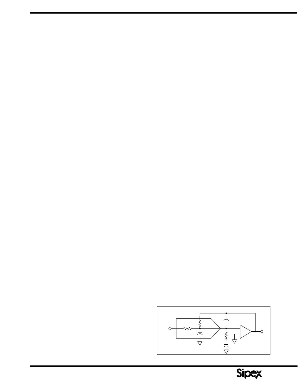
Cf
Rf
VREF
–
Ri
CO
Rp
+
EO
C
Figure 1. SP7514/HS3140 Equivalent Output Circuit
Corporation
SIGNAL PROCESSING EXCELLENCE
Share Link: 