HSP43891 データシートの表示(PDF) - Intersil
部品番号
コンポーネント説明
メーカー
HSP43891 Datasheet PDF : 18 Pages
| |||
HSP43891
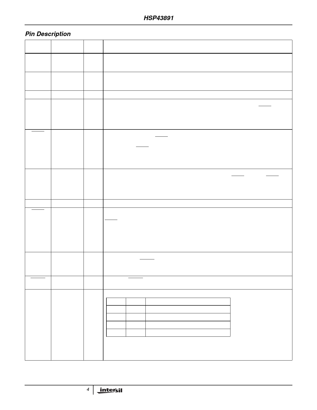
Pin Description
SYMBOL
VCC
VSS
CLK
DIN0-8
PIN
NUMBER
B1, J1, A3, K4,
L7, A10, F10,
D11
A1, F1, E2, K3,
K6, L9, A11,
F11, J11
G3
A5-8, B5-7, C6,
C7
DIENB
C5
CIN0-8
A9, B9-11, C10,
C11, D10, E9,
E10
ALIGN PIN
C3
CIENB
B8
COUT0-8
B2, B3, C1, D1,
E1, C2, D2, F2,
E3
COENB
A2
DCM0-1
L1, G2
TYPE
I
I
I
I
I
O
I
I
+5 power supply input.
NAME AND FUNCTION
Power supply ground input.
The CLK input provides the DF system sample clock. The maximum clock frequency is 30MHz.
These nine inputs are the data sample input bus. Nine-bit data samples are synchronously loaded
through these pins to the X register of each filter cell of the DF simultaneously. The DIENB signal en-
ables loading, which is synchronous on the rising edge of the clock signal.
The data samples can be either 9-bit two’s complement or 8-bit unsigned values. For 9-bit two’s com-
plement values, DIN8 is the sign bit. For 8-bit unsigned values, DIN8 must be held at logical zero.
A low on this input enables the data sample input bus (DIN0-8) to all the filter cells. A rising edge of the
CLK signal occurring while DIENB is low will load the X register of every filter cell with the 9-bit value
present on DIN0-8. A high on this input forces all the bits of the data sample input bus to zero; a rising
CLK edge when DIENB is high will load the X register of every filter cell with all zeros. This signal is
latched inside the device, delaying its effect by one clock internal to the device. Therefore it must be low
during the clock cycle immediately preceding presentation of the desired data on the DIN0-8 inputs. De-
tailed operation is shown in later timing diagrams.
These nine inputs are used to input the 9-bit coefficients. The coefficients are synchronously loaded
into the C register of filter CELL0 if a rising edge of CLK occurs while CIENB is low. The CIENB signal
is delayed by one clock as discussed below.
The coefficients can be either 9-bit two’s complement or 8-bit unsigned values. For 9-bit two’s comple-
ment values, CIN8 is the sign bit. For 8-bit unsigned values, CIN8 must be held at logical zero.
Used for aligning chip on socket or printed circuit board. This pin must be left as a no connect in circuit.
A low on this input enables the C register of every filter cell and the D (decimation) registers of every
filter cell according to the state of the DCM0-1 inputs. A rising edge of the CLK signal occurring while
CIENB is low will load the C register and appropriate D registers with the coefficient data present at
their inputs. This provides the mechanism for shifting coefficients from cell to cell through the device. A
high on this input freezes the contents of the C register and the D registers, ignoring the CLK signal.
This signal is latched and delayed by one clock internal to the DF. Therefore it must be low during the
clock cycle immediately preceding presentation of the desired coefficient on the CIN0-8 inputs. Detailed
operation is shown in later timing diagrams.
These nine three-state outputs are used to output the 9-bit coefficients from filter CELL7. These outputs
are enabled by the COENB signal low. These outputs may be tied to the CIN0-8 inputs of the same DF
to recirculate to coefficients, or they may be tied to the CIN0-8 inputs of another DF to cascade DFs for
longer filter lengths.
A low on the COENB input enables the COUT0-8 outputs. A high on this input places all these outputs
in their high impedance state.
These two inputs determine the use of the internal decimation registers as follows:
DCM1 DCM0
DECIMATION FUNCTION
0
0 Decimation registers not used
0
1 One decimation register is used
1
0 Two decimation registers are used
1
1 Three decimation registers are used
The coefficients pass from cell to cell at a rate determined by the number of decimation registers used.
When no decimation registers are used, coefficients move from cell to cell on each clock. When one
decimation register is used, coefficients move from cell to cell on every other clock, etc. These signals
are latched and delayed by one clock internal to the device.
4
Share Link: 