HT46R343 データシートの表示(PDF) - Holtek Semiconductor
部品番号
コンポーネント説明
メーカー
HT46R343 Datasheet PDF : 40 Pages
| |||
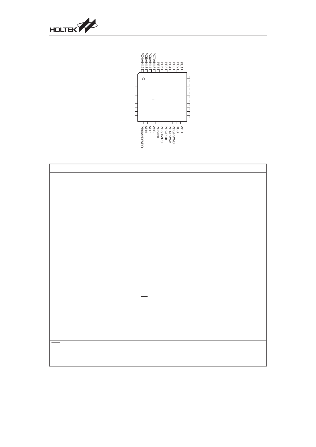
Pin Assignment
P C 3 /A N 1 1
P C 2 /A N 1 0
P C 1 /A N 9
P C 0 /A N 8
P B 7 /A N 7
P B 6 /A N 6
P B 5 /A N 5
P B 4 /A N 4
P B 3 /A N 3
P B 2 /A N 2
P B 1 /A N 1
44 43 42 41 40 39 38 37 36 35 34
1
33
2
32
3
31
4
30
5
6
7
H T46R 343
4 4 Q F P -A
29
28
27
8
26
9
25
10
24
11
23
12 13 14 15 16 17 18 19 20 21 22
PE0
PA7
PA6
PA5
P A 4 /T R M 1
P A 3 /P F D
PA2
PA1
PA0
O SC2
O SC1
HT46R343
Pin Description
Pin Name I/O Options
Description
PA0~PA2
PA3/PFD
PA4/TMR1
PA5~PA7
Pull-high Bidirectional 8-bit input/output port. Each pin can be configured as wake-up
Wake-up input by configuration options. Software instructions determine if the pin is a
I/O
PA3 or PFD
Timer 0 or
CMOS output or Schmitt trigger input. Configuration options determine which
pins on the port have pull-high resistors. The PFD and TMR1 pins are
Timer 1 (PFD pin-shared with PA3 and PA4.
Clock Source) PA0~PA7 can be used as LED driver (source end).
PB0/AN0/APO,
PB1/AN1~
PB7/AN7,
I/O
PC0/AN8~
PC7/AN15
Pull-high
16 lines AD inut pun-shared with PB and PC.
Bidirectional 8-bit input/output port. Software instructions determine if the
pin is a CMOS output or Schmitt trigger input. Configuration options determine
which pins on the port have pull-high resistors. Pins PB, PC are pin-shared
with the A/D input pins. The A/D inputs are selected via software instructions.
Once selected as an A/D input, the I/O function and pull-high resistor are dis-
abled automatically.
About PB0/AN0/APO: If the pin is PB0 (setting by ADCS.PCR3~0=00), ADC
and OP amp should be power off automatically.
If the pin is AN0 (setting by ADCS.PCR3~0), APO is connected with AN0 pin
together and OP amp on/off is controlled by OPAC.OPAEN.
PD0/PWM0
PD1/PWM1
PD2/PCK
PD5/TMR0
PD6/INT
Bi-directional 4-bit input/output port. Software instructions determine if the
Pull-high pin is a CMOS output or Schmitt trigger input. Configuration options determine
I/O
PD0 or PWM0
PD1 or PWM1
which pins on this port have pull-high resistors. PD0/PD1 are pin-shared with
the PWM0/PWM1 outputs selected via configuration option.
PD2 or PCK PD0, PD1, PD2, PD5, PD6 are pin-shared with the PWM0, PWM1, PCK,
TMR0, INT output selected via configuration option.
PE0~PE7
Bidirectional 8-bit input/output port. Software instructions determine if the
I/O
Pull-high
pin is a CMOS output or Schmitt trigger input. A configuration option deter-
mines if all pins on the port have pull-high resistors.
PE0~PE7 can be used as LED driver (sink end).
APN
APP
I
I
¾
APN and APP are the internal operational amplifier, negative input pin and
positive input pin respectively .
RES
I
¾
Schmitt trigger reset input. Active low.
VDD
¾
¾
Positive power supply
VSS
¾
¾
Negative power supply, ground.
Rev. 1.00
3
October 11, 2007
Share Link: 