HT82K68 データシートの表示(PDF) - Holtek Semiconductor
部品番号
コンポーネント説明
メーカー
HT82K68 Datasheet PDF : 39 Pages
| |||
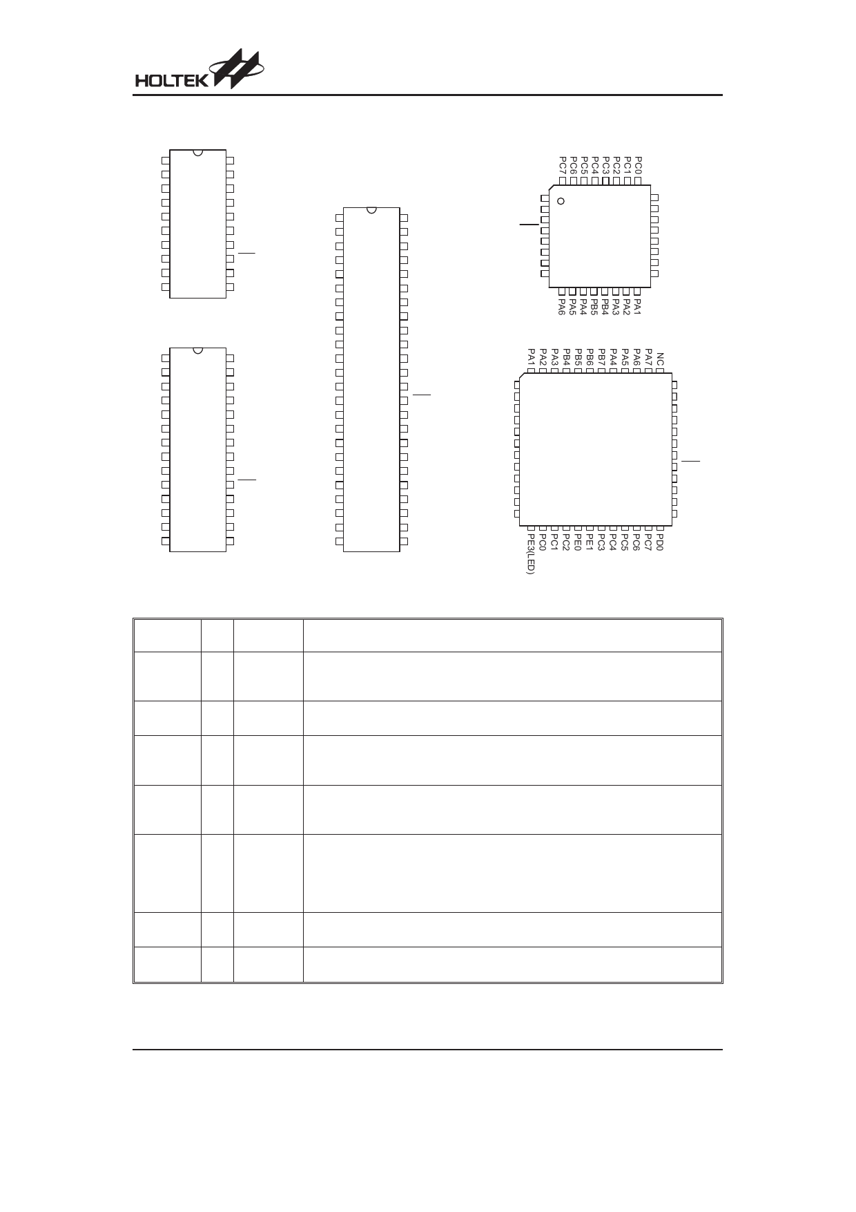
HT82K68E-L/HT82K68A-L
Pin Assignment
PA3 1
PA2 2
PA1 3
PA0 4
PB1 5
PB0 6
VSS 7
PE2 8
PC0 9
P C 1 10
20 P A 4
19 P A 5
18 P A 6
17 P A 7
16 O S C 2
15 O S C 1
14 V D D
13 R E S
12 P C 3
11 P C 2
H T 8 2 K 6 8 E -L /H T 8 2 K 6 8 A -L
2 0 S O P -A
PB5 1
PB4 2
PA3 3
PA2 4
PA1 5
PA0 6
PB3 7
PB2 8
PB1 9
P B 0 10
V S S 11
P C 1 12
P C 2 13
P C 3 14
28 P B 6
27 P B 7
26 P A 4
25 P A 5
24 P A 6
23 P A 7
22 O S C 2
21 O S C 1
20 V D D
19 R E S
18 P C 7
17 P C 6
16 P C 5
15 P C 4
H T 8 2 K 6 8 E -L /H T 8 2 K 6 8 A -L
2 8 S O P -A
PB5 1
PB4 2
PA3 3
PA2 4
PA1 5
PA0 6
PB3 7
PB2 8
PB1 9
P B 0 10
N C 11
N C 12
P D 7 13
P D 6 14
P D 5 15
P D 4 16
V S S 17
P E 2 (L E D ) 1 8
P E 3 (L E D ) 1 9
P C 0 20
P C 1 21
P C 2 22
P E 0 23
P E 1 24
48 P B 6
47 P B 7
46 P A 4
45 P A 5
44 P A 6
43 P A 7
42 N C
41 N C
40 N C
39 N C
38 O S C 2
37 O S C 1
36 V D D
35 R E S
3 4 P E 4 (L E D )
33 P D 3
32 P D 2
31 P D 1
30 P D 0
29 P C 7
28 P C 6
27 P C 5
26 P C 4
25 P C 3
H T 8 2 K 6 8 E -L /H T 8 2 K 6 8 A -L
4 8 S S O P -A
32 31 30 29 28 27 26 25
PD0 1
24 V S S
PD1 2
23 P D 4
PD2 3
RES 4
VDD 5
O SC1 6
22 P D 5
H T 8 2 K 6 8 E -L
H T 8 2 K 6 8 A -L
3 2 Q F N -B
21
20
19
PB0
PB1
PB2
O SC2 7
18 P B 3
PA7 8
17 P A 0
9 10 11 12 13 14 15 16
PA0
PB3
PB2
PB1
PB0
PD7
PD6
PD5
PD4
VSS
P E 2 (L E D )
NC
1
48
47
46
45
44
43
42
41
40
39
38
37
36
2
35
3
34
4
33
5
32
6
7
8
H T 8 2 K 6 8 E -L
H T 8 2 K 6 8 A -L
4 8 L Q F P -A
31
30
29
9
28
10
27
11
26
12
25
13 14 15 16 17 18 19 20 21 22 23 24
NC
NC
NC
NC
O SC2
O SC1
VDD
RES
P E 4 (L E D )
PD3
PD2
PD1
Pin Description
Pin Name I/O
Mask
Option
Description
Wake-up Bidirectional 8-bit input/output port. Each bit can be configured as a wake-up input
PA0~PA7 I/O Pull-high by mask option. Software* instructions determine the CMOS output or Schmitt
or None Trigger input with or without 12K pull-high resistor.
PB0~PB7
I/O
Pull-high Bidirectional 8-bit input/output port. Software* instructions determine the output or
or None Schmitt Trigger input with or without pull-high resistor.
Wake-up This pin is an I/O port. NMOS open drain output with pull-high resistor and can be
PC0
I/O Pull-high used as DATA or CLOCK line of PS2. This pin can be configured as a wake-up
or None input by mask option.
Wake-up This pin is an I/O port. NMOS open drain output with pull-high resistor and can be
PC1
I/O Pull-high used as DATA or CLOCK line of PS2. This pin can be configured as a wake-up
or None input by mask option.
Bidirectional 2-bit input/output port. Each bit can be configured as a wake-up input
Wake-up by mask option. Software* instructions determine the CMOS output or Schmitt
PC2~PC3 I/O Pull-high Trigger input with or without pull-high resistor.
or None PC2 also as external interrupt input pin. PE0 determine whether rising edge or
falling edge of PC2 to trigger the INT circuit.
PC4~PC7
I/O
Pull-high Bidirectional 4-bit input/output port. Software* instructions determine the CMOS
or None output or Schmitt Trigger input with or without pull-high resistor.
PD0~PD7
I/O
Pull-high Bidirectional 8-bit input/output port. Software* instructions determine the CMOS
or None output or Schmitt Trigger input with or without pull-high resistor.
Rev. 1.40
3
February 1, 2011
Share Link: 