HT82K68 データシートの表示(PDF) - Holtek Semiconductor
部品番号
コンポーネント説明
メーカー
HT82K68 Datasheet PDF : 39 Pages
| |||
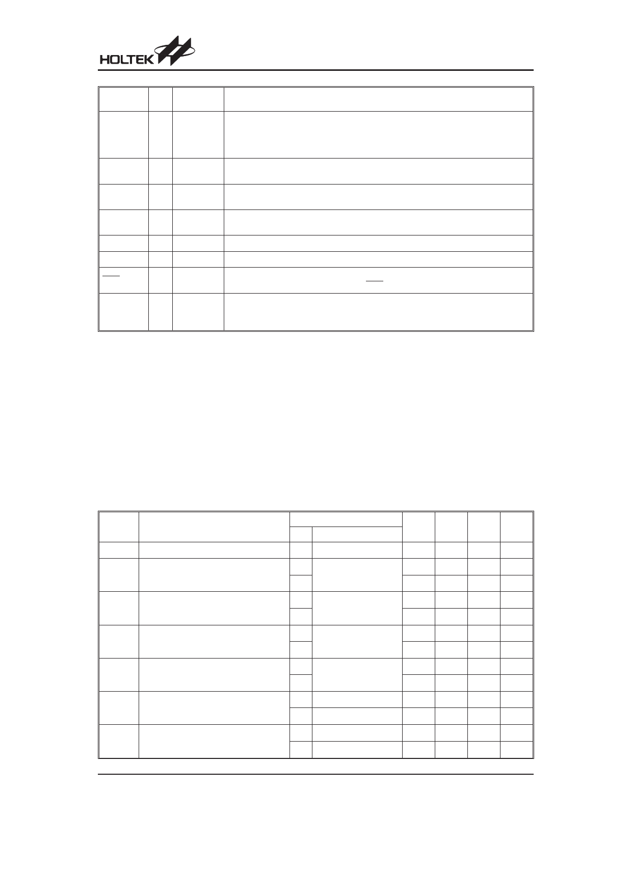
HT82K68E-L/HT82K68A-L
Pin Name I/O
Mask
Option
Description
Bidirectional input/output port. Software* instruction determine the CMOS output
PE0~PE1
I/O
Pull-high or Schmitt Trigger input with or without pull-high resistor.
or None If PE0 output 1, rising edge of PC2 trigger INT circuit.
PE0 output 0, falling edge of PC2 trigger INT circuit.
PE2
O
This pin is a CMOS output structure. The pad can function as LED (SCR) drivers
for the keyboard. IOL=18mA at VOL=3.4V
PE3
O
This pin is a CMOS output structure. The pad can function as LED (NUM) drivers
for the keyboard. IOL=18mA at VOL=3.4V
PE4
O
This pin is a CMOS output structure. The pad can function as LED (CAP) drivers for
the keyboard. IOL=18mA at VOL=3.4V
VDD
¾
¾
Positive power supply
VSS
RES
OSC1
OSC2
¾
¾
Negative power supply, ground
I
¾
Chip reset input. Active low. Built-in power-on reset circuit to reset the entire chip.
Chip can also be externally reset via RES pin
OSC1, OSC2 are connected to an RC network or a crystal for the internal system
I Crystal or clock. In the case of RC operation, OSC2 is the output terminal for the 1/4 system
O
RC
clock; A 110kW resistor is connected to OSC1 to generate a 2 MHZ frequency.
Note: *: Software means the HT-IDE (Holtek Integrated Development Environment) can be configured by mask
option.
Absolute Maximum Ratings
Supply Voltage ..........................VSS-0.3V to VSS+6.0V
Input Voltage .............................VSS-0.3V to VDD+0.3V
Storage Temperature ...........................-50°C to 125°C
Operating Temperature ..........................-25°C to 70°C
Note: These are stress ratings only. Stresses exceeding the range specified under ²Absolute Maximum Ratings² may
cause substantial damage to the device. Functional operation of this device at other conditions beyond those
listed in the specification is not implied and prolonged exposure to extreme conditions may affect device
reliability.
D.C. Characteristics
Symbol
Parameter
VDD
Operating Voltage
IDD1
Operating Current (Crystal OSC)
IDD2
Operating Current (RC OSC)
ISTB1
Standby Current (WDT enabled)
ISTB2
Standby Current (WDT Disabled)
VIL1
Input Low Voltage for I/O Ports
(Schmitt)
VIH1
Input High Voltage for I/O Ports
(Schmitt)
Ta=25°C
Test Conditions
VDD
Conditions
Min. Typ. Max. Unit
¾
¾
1.8
¾
5.5
V
3V
¾
No load, fSYS= 6MHz
5V
¾
0.7 1.5 mA
2
5
mA
3V
¾
No load, fSYS= 6MHz
5V
¾
0.5 1.5 mA
2
5
mA
3V
¾
¾
8
mA
No load, system HALT
5V
¾
¾
15
mA
3V
¾
¾
3
mA
No load, system HALT
5V
¾
¾
6
mA
3V
¾
0
¾ 0.3VDD V
5V
¾
0
¾ 0.3VDD V
3V
¾
0.7VDD ¾
VDD
V
5V
¾
0.7VDD ¾
VDD
V
Rev. 1.40
4
February 1, 2011
Share Link: 