HT82V26 データシートの表示(PDF) - Holtek Semiconductor
部品番号
コンポーネント説明
メーカー
HT82V26 Datasheet PDF : 16 Pages
| |||
HT82V26
D8
D7
D6
D5
D4
D3
D2
D1
D0
3 channels CDS operation Clamp bias Power-down
Set to 0 Set to 0 Set to 1
1=On*
1=CDS mode* 1=4V*
1=On
1 byte out
Output delay (High-byte
only)
1=On
1=On
0=Off
0=SHA mode 0=3V
0=Off (Normal)* 0=Off*
0=Off*
Configuration Register Settings
Note: * Power-on default value
MUX Register
The MUX register controls the sampling channel order and the 2-channel mode configuration in the HT82V26. Bits D8
should always be set low. Bit D7 is used when operating in the 3-channel mode or the 2-channel mode. Setting bit D7
high will sequence the MUX to sample the red channel first, then the green channel, and then the blue channel. When
in the 3-channel mode, the CDSCLK2 rising edge always resets the MUX to sample the red channel first (see timing di-
agrams). When bit D7 is set low, the channel order is reversed to blue first, green second, and red third. The CDSCLK2
rising edge will always reset the MUX to sample the blue channel first. Bits D6, D5 and D4 are used when operating in 1
or 2-channel mode. Bit D6 is set high to sample the red channel. Bit D5 is set high to sample the green channel. Bit D4
is set high to sample the blue channel. The MUX will remain stationary during 1-channel mode. The two channel mode
is selected by setting two of the channel select bits (D4~D6) high. The MUX samples the channels in the order selected
by bit D7. Bits D0~D3 are used for controlling CDSCLK1, CDSCLK2 and ADCCLK internal delay.
D8
D7
D6
D5
D4
D3
D2
D1
D0
MUX Order
Channel Select
Enable Delay CDS1 Delay CDS2 Delay ADCK Delay
Set to 0 1=R-G-B* 1=RED* 1=GREEN 1=BLUE
0=B-G-R 0=Off 0=Off* 0=Off*
0=Off
1=On*
0=2ns*
1=4ns
0=2ns*
1=4ns
0=0ns*
1=2ns
MUX Register Settings
Note: * Power-on default value
PGA Gain Registers
There are three PGA registers for use in individually programming the gain in the red, green and blue channels. Bits D8,
D7 and D6 in each register must be set low, and bits D5 through D0 control the gain range in 64 increments. See figure
for a graph of the PGA gain versus PGA register code. The coding for the PGA registers is a straight binary, with an all
zero words corresponding to the minimum gain setting (1x) and an all one word corresponding to the maximum gain
setting (5.85x).
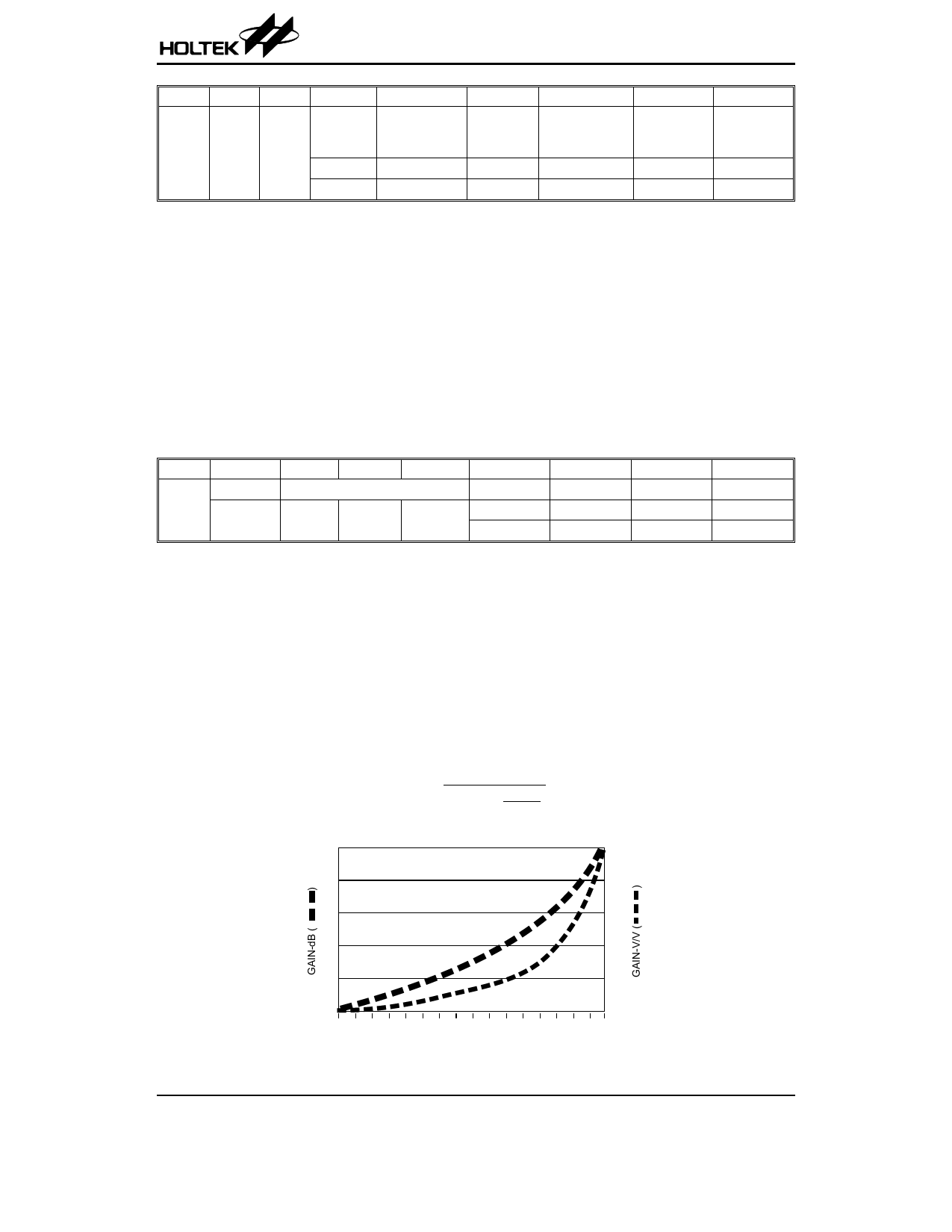
The HT82V26 uses one Programmable Gain Amplifier (PGA) for each channel. Each PGA has a gain range from 1x
(0dB) to 5.85x (15.3dB), adjustable in 64 steps. The Figure shows the PGA gain as a function of the PGA register code.
Although the gain curve is approximately linear in dB, the gain in V/V varies in nonlinear proportion with the register
code, according to the following the equation: Gain=
1+
5.85
4.85 ´´ ( 63 -
G)
63
Where G is the decimal value of the gain register contents, and varies from 0 to 63.
15
5 .8 5
12
5 .0
9
4 .0
6
3 .0
3
2 .0
0
1 .0
0 4 8 12 16 20 24 28 32 36 40 44 48 52 56 60 63
P G A r e g is te r v a lu e - - D e c im a l
PGA Gain Transfer Function
Rev. 1.50
6
June 24, 2004
Share Link: 