HT82V42 データシートの表示(PDF) - Holtek Semiconductor
部品番号
コンポーネント説明
メーカー
HT82V42 Datasheet PDF : 24 Pages
| |||
HT82V42
Input Sampling Block: Input Sampling and Referencing
If CDS = 1, (i.e. CDS operation) the previously sampled reset level, VRESET, is subtracted from the input video.
V1 = VIN - VRESET...................................................................Eqn. 1
If CDS = 0, (non-CDS operation) the simultaneously sampled voltage on pin VRLC is subtracted instead.
V1 = VIN - VVRLC .....................................................................Eqn. 2
If VRLCEXT = 1, VVRLC is an externally applied voltage on pin VRLC/VBIAS.
If VRLCEXT = 0, VVRLC is the output from the internal RLC DAC.
VVRLC = (VRLCSTEP ´ RLCV[3:0]) + VRLCBOT....................Eqn. 3
VRLCSTEP is the step size of the RLC DAC and VRLCBOT is the minimum output of the RLC DAC.
OFFSET DAC Block: OFFSET (BLACK - LEVEL) Adjust
The resultant signal V1 is added to the Offset DAC output.
V2 = V1 + { 315mV ´ (DAC[7:0] - 127.5) } / 127.5.....................Eqn. 4
PGA NODE: GAIN Adjust
The signal is then multiplied by the PGA gain,
V3 = V2 ´ [186 / (278 - PGA[7:0] ) ]...........................................Eqn. 5
ADC Block: Analogue-Digital Conversion
The analogue signal is then converted to a 16-bit unsigned number, with input range configured by PGAFS[1:0].
D1[15:0] = INT{ (V3 /VFS) ´ 65535} + 32767 PGAFS[1:0] = 00 or 01 .................Eqn. 6
D1[15:0] = INT{ (V3 /VFS) ´ 65535}
PGAFS[1:0] = 11 ..........................Eqn. 7
D1[15:0] = INT{ (V3 /VFS) ´ 65535} + 65535 PGAFS[1:0] = 10 ..........................Eqn. 8
where the ADC full-scale range, VFS = 2.0V
if D1[15:0] < 0
D1[15:0] = 0
if D1[15:0] > 65535 D1[15:0] = 65535
Output Invert Block: Polarity Adjust
The polarity of the digital output may be inverted by control bit INVOP.
D2[15:0] = D1[15:0]
(INVOP = 0).....................................................Eqn. 9
D2[15:0] = 65535 - D1[15:0]
(INVOP = 1)...................................................Eqn. 10
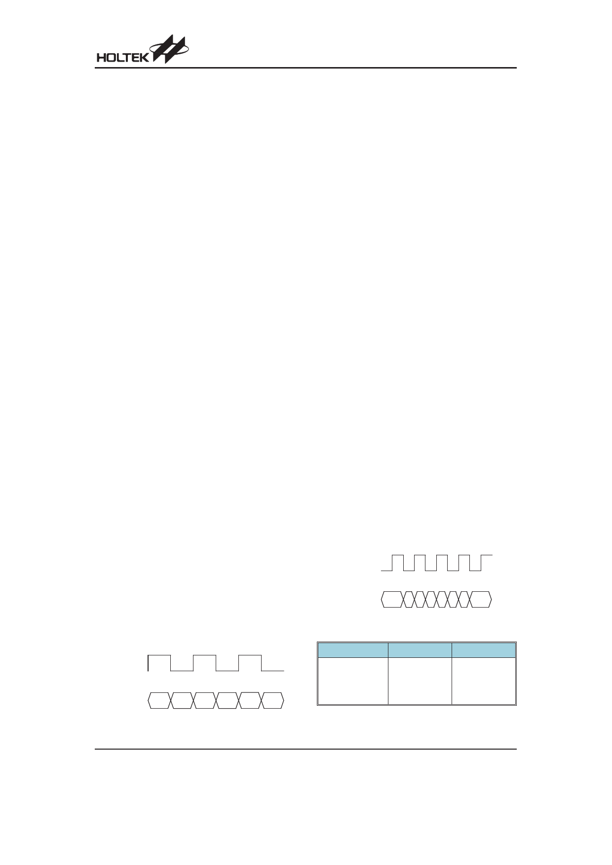
Output Formats
Latency of valid output data with respect to CDSCLK2 is
programmable by writing to control bits DEL[1:0]. The
latency for each mode is shown in the Operating Mode
Timing Diagrams section. Figure shows the output data
formats for Modes 1, 3 and 4. Figure shows the output
data formats for Mode 2. Table summarizes the output
data obtained for each format.
M C LK
4 + 4 + 4 + 4 - B it
O u tp u t
A
B
C
D
Output Data Formats (Mode 1, 3, 4)
M C LK
4 + 4 + 4 + 4 - B it
O u tp u t
ABABCD
Output Data Formats (Mode 2)
Output Format Output Pins
Output
4+4+4+4-Bit
(Nibble)
OD3~OD0
A= d15~d12
B= d11~d8
C= d7~d4
D= d3~d0
Details of Output Data
Rev. 1.20
11
December 8, 2010
Share Link: 