HT9252 データシートの表示(PDF) - Holtek Semiconductor
部品番号
コンポーネント説明
メーカー
HT9252 Datasheet PDF : 15 Pages
| |||
HT9251/HT9252/HT9254
Absolute Maximum Ratings
Supply Voltage ......................................................6.0V
Input voltage range ..................VSS–0.3V to VDD+0.3V
Differential Input Voltage ........................ ±(VDD – VSS)
ESD protection - all pins (HBM;MM) .....≥4kV; 200V
Storage Temperature ........................... -65°C to 150°C
Operating Temperature.......................... -40°C to 85°C
Junction Temperature......................................... 150°C
Note: These are stress ratings only. Stresses exceeding the range specified under "Absolute Maximum Ratings"
may cause substantial damage to the device. Functional operation of this device at other conditions beyond
those listed in the specification is not implied and prolonged exposure to extreme conditions may affect
device reliability.
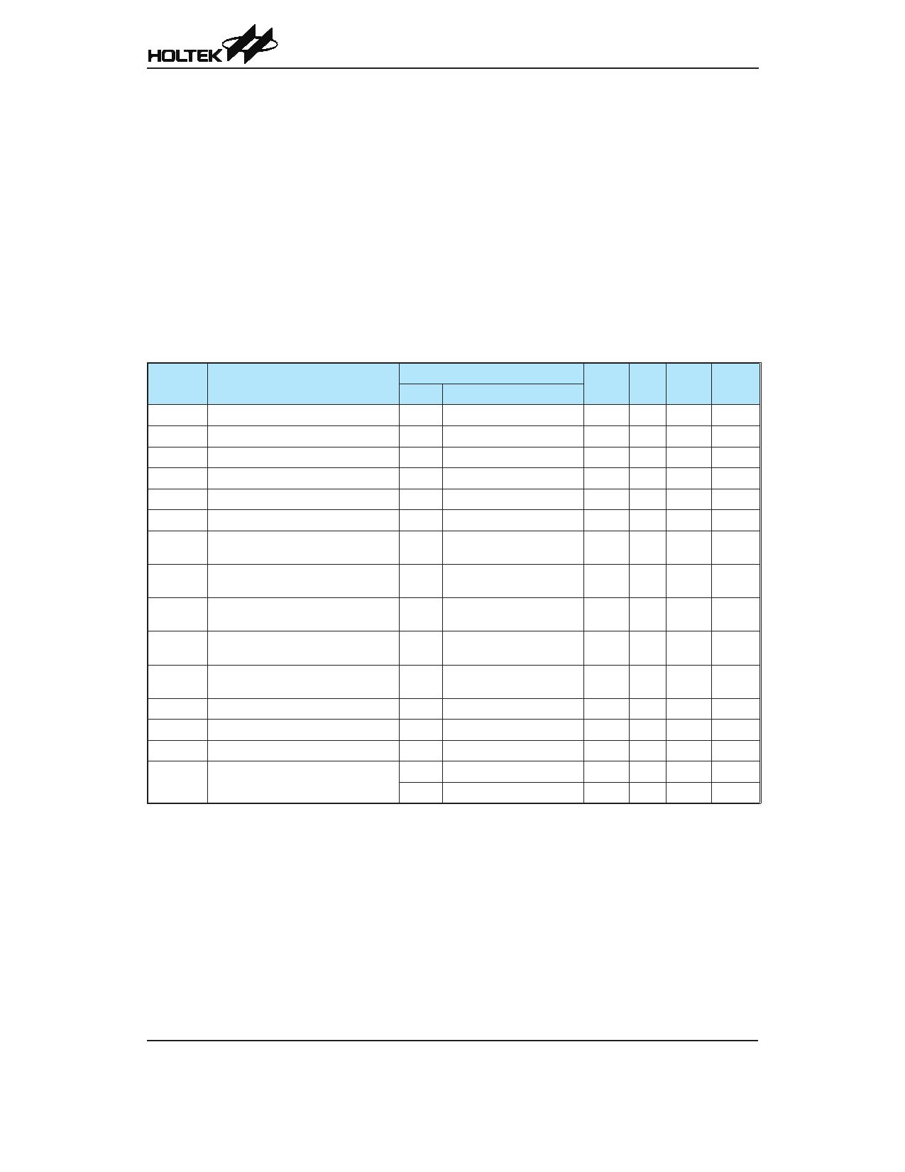
Electrical Characteristics
Unless otherwise indicated, VSS=GND, TA = 25°C, VCM = VDD/2, VOUT ≈VDD/2, VL=VDD/2, and RL=100kΩ to VL, CL =60pF.
Symbol
VDD
VOS
ΔVOS/ΔT
IOS
IB
VCM
VOH, VOL
AOL
GBW
Фm
CMRR
PSRR
ICC
SR
ISC
Parameter
Supply Voltage
Input Offset Voltage
Temperature Drift
Input Offset Current
Input Bias Current
Input Common Mode Range
Maximum Output Voltage Swing
DC Open-Loop Gain - Large Signal
Gain Bandwidth Product
Phase Margin
Common Mode Rejection Ratio
Power Supply Rejection Ratio
Supply Current per Single Amplifier
Slew Rate at Unity Gain
Output Short Circuit Current
VDD
—
5V
5V
5V
5V
5V
5V
5V
5V
5V
5V
5V
5V
5V
1.8V
5.5V
Test Conditions
Conditions
Min.
—
1.8
VCM=0~3V
-6
VIN=VCM/2
—
TA=25°C
—
TA=25°C
—
TA=25°C
VSS+20
0.5V input overdrive
RL=100kΩ to VL
VSS+35
VOUT=35mV to VDD−35mV
VIN=VCM/2
70
RL=10kΩ, CL=60pF,
VIN=VCM/2
—
RL=10kΩ, CL=60pF
G=+1V/V, VIN+= VDD/2
—
VCM = VSS+20mV to VDD-
20mV
VIN=0.2V
65
Io=0A
30
RL=100kΩ, CL=60pF
—
—
—
Typ.
—
—
±2
±5
±50
—
—
100
550
68
75
95
50
0.3
±6
±23
Max. Unit
5.5
+6
—
—
—
VDD-20
V
mV
uV/°C
pA
pA
mV
VDD-35 mV
—
dB
—
kHz
— Degree
—
dB
—
dB
70
uA
— V/µs
--
mA
--
mA
Rev. 1.00
3
December 14, 2012
Share Link: 