HT9291 データシートの表示(PDF) - Holtek Semiconductor
部品番号
コンポーネント説明
メーカー
HT9291 Datasheet PDF : 14 Pages
| |||
HT9291/HT9292/HT9294
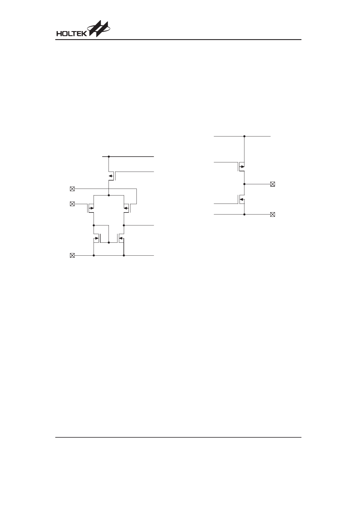
Functional Description
Input Stage
The input stage of op amps are nominal PMOS differen-
tial amplifiers (see the following diagram), therefore the
common mode input voltage can extend to VSS-0.6V.
On the other hand the common mode input voltage has
to be maintained below (VDD-1.2V) to keep the input de-
vice (M2 and M3) active. This implies that when using
HT9291/HT9292/HT9294 as a voltage follower, the in-
put as well as output active range will be limited be-
tween VSS~VDD-1V (approx.). Avoid applying any
voltage greater than VDD+0.6V or less than VSS-0.6V to
the input pins, otherwise the internal input protection de-
vices may be damaged.
V DD
V B IA S
M1
N o n in v e r tin g In
In v e r tin g In
M2
PM O S
M3
PM O S
T o O u tp u t S ta g e
M4
V SS
M5
V SS
Since the input impedance of PMOS is inherently very
high, it can directly couple to high impedance elements
without loading effect. For example, coupling to ceramic
transducers, integrating capacitor and resistor net-
works.
Actually the extremly high input impedance is its major
advantage over the bipolar counterpart, in some appli-
cation fields such as integrators where the input current
of op amp can cause significant error.
Output Stage
The HT9291/HT9292/HT9294 uses push-pull CMOS
configuration as the output stage of op amps to mini-
mize low power consumption and to provide adequate
output driving current.
Note that the output is an unbuffered structure, therefore
the open loop gain will be affected by the load resistor
since the voltage gain of this stage can be expressed as
(gm5+ gm6)´RL.
V DD
V B IA S
F ro m
D iffe r e n tia l
Am p
M5
OUT
M6
V SS
Because of the consideration for minimized power con-
sumption, the output short circuit current is limited to
about -1.2mA for source drive and 4mA for sink drive.
This is believed to be enough for most low power sys-
tems, however it is recommended to use the load resis-
tor of >1MW for normal applications. In case of heavy
load driving, an external buffer stage using bipolar tran-
sistors is recommended.
The HT9291/HT9292/HT9294 is internally compen-
sated for AC stability and capable to withstand up to a
60pF capacitive load.
Rev. 1.10
4
October 12, 2010
Share Link: 