HT9315 データシートの表示(PDF) - Holtek Semiconductor
部品番号
コンポーネント説明
メーカー
HT9315 Datasheet PDF : 27 Pages
| |||
HT9315 Series
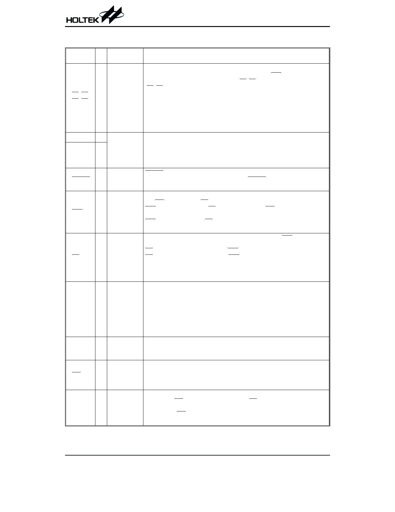
Pin Description
Pin Name
I/O
Internal
Connection
Description
C1~C5
R1~R4
I/O
CMOS
IN/OUT
These pins form a 4´5 keyboard matrix which can perform keyboard input detection
and dialing specification setting functions. When on-hook (HKS=high) all the pins are
set high. While off-hook the column group (C1~C5) remains low and the row group
(R1~R4) is set high for key input detection.
An inexpensive single contact 4´5 keyboard can be used as an input device.
Pressing a key connects a single column to a single row, and actuates the system os-
cillator that results in a dialing signal output. If more than two keys are pressed at the
same time, no response occurs. The key-in debounce time is 20ms. Refer to the key-
board information for keyboard arrangement and to the functional description for dial-
ing specification selection.
X1
I
The system oscillator consists of an inverter, a bias resistor and the necessary
load capacitor on chip. Connecting a standard 3.579545MHz crystal or ceramic
OSCILLATOR resonator to the X1 and X2 terminals can implement the oscillator function. The
X2
O
oscillator is turned off in the standby mode, and is actuated whenever a keyboard
entry is detected.
XMUTE is an NMOS open drain structure pulled to VSS during dialing signal
XMUTE O NMOS OUT transmission. Otherwise, it is an open circuit. XMUTE is used to mute the speech
circuit when transmitting the dial signal.
HKS
This pin is used to monitor the status of the hook-switch and its combination with
HFI/HDI can control the PO pin output to make or break the line.
I
CMOS IN
HKS=VDD: On-hook state (PO=low). Except for HFI/HDI
(hand-free/hold-line control input), other functions are all disabled.
HKS=VSS: Off-hook state (PO=high). The chip is in the standby mode and ready to
receive the key input.
This pin is a CMOS output structure which by receiving the HKS and HFO/HDO
signals, control the dialer to connect or disconnect the telephone line.
PO outputs a low to break line when HKS is high (on-hook) and HFO/HDO is low.
PO
O CMOS OUT PO outputs a high to make line when HKS is low (off-hook) or HFO is high or HDO
is high.
During the off-hook state, this pin also outputs the dialing pulse train in pulse
mode dialing. While in the tone mode, this pin is always high.
MODE I/O
CMOS
IN/OUT
This is a three-state input/output pin, use for dialing mode selection, either Tone
mode or Pulse mode, 10pps/20pps
MODE=VDD: Pulse mode, 10pps
MODE=OPEN: Pulse mode, 20pps
MODE=VSS: Tone mode
During the pulse mode dialing, switching this pin to the tone mode changes the
subsequent digit entry to tone mode. When the chips are in tone mode, switching
to pulse mode will also be recognized.
DTMF
This pin is active only when the chip transmits tone dialing signals. Otherwise, it
O CMOS OUT always outputs a low. The pin outputs tone signals to drive the external transmitter
amplifier circuit. The load resistor should not be less than 5kW.
This pin is a Schmitt trigger input structure. Active low. Applying a negative going
HDI
I
CMOS IN pulse to this pin can toggle the HDO output once.
Pull-High An external RC network is recommended for input debouncing. The pull-high re-
sistance is 200kW typ.
HDO
The HDO is a CMOS output structure. Its output is toggle- controlled by a negative
transition on HDI. When HDO is toggled high, PO keeps high to hold the line. The
O CMOS OUT hold function can be released by setting HFO high or by an on/off hook operation
or by another HDI input. Refer to the functional description for the hold-line func-
tion.
Rev. 1.20
3
October 1, 2002
Share Link: 