HT82K96A データシートの表示(PDF) - Holtek Semiconductor
部品番号
コンポーネント説明
メーカー
HT82K96A Datasheet PDF : 46 Pages
| |||
HT82K96A
At a subroutine call or interrupt acknowledge signal, the
contents of the program counter are pushed onto the
stack. At the end of a subroutine or an interrupt routine,
signaled by a return instruction (RET or RETI), the pro-
gram counter is restored to its previous value from the
stack. After a chip reset, the SP will point to the top of the
stack.
If the stack is full and a non-masked interrupt takes
place, the interrupt request flag will be recorded but the
acknowledge signal will be inhibited. When the stack
pointer is decremented (by RET or RETI), the interrupt
will be serviced. This feature prevents stack overflow al-
lowing the programmer to use the structure more easily.
In a similar case, if the stack is full and a ²CALL² is sub-
sequently executed, stack overflow occurs and the first
entry will be lost (only the most recent 8 return ad-
dresses are stored).
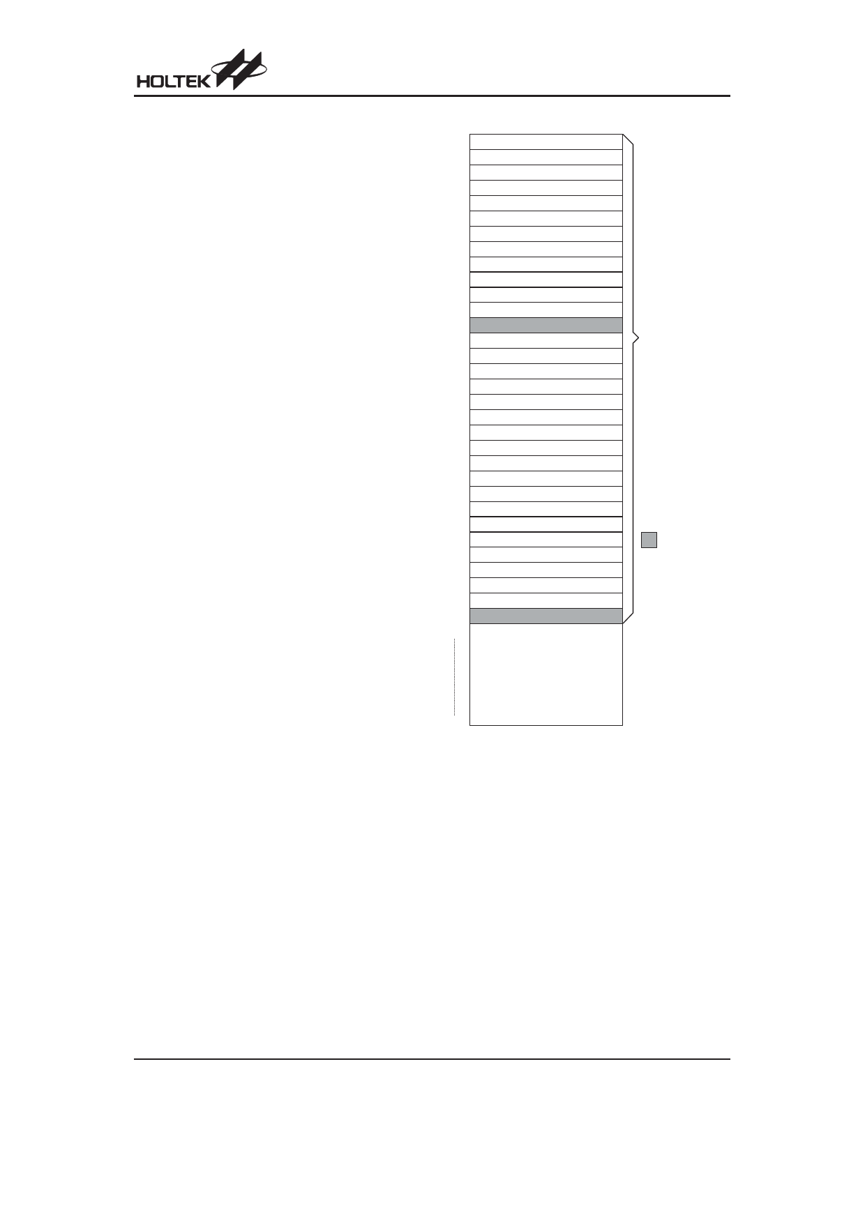
Data Memory - RAM for Bank 0
The data memory is designed with 190´8 bits. The
data memory is divided into two functional groups: spe-
cial function registers and general purpose data mem-
ory (160´8). Most are read/write, but some are read
only.
The special function registers include the indirect ad-
dressing registers (R0;00H, R1;02H), Bank register
(BP, 04H), Timer/Event Counter 0 (TMR0;0DH),
Timer/Event Counter 0 control register (TMR0C;0EH),
Timer/Event Counter 1 higher order byte register
(TMR1H;0FH), Timer/Event Counter 1 lower order byte
register (TMR1L;10H), Timer/Event Counter 1 control
register (TMR1C;11H), program counter lower-order
byte register (PCL;06H), memory pointer registers
(MP0;01H, MP1;03H), accumulator (ACC;05H), table
pointer (TBLP;07H), table higher-order byte register
(TBLH;08H), status register (STATUS;0AH), interrupt
control register (INTC;0BH), Watchdog Timer option
setting register (WDTS;09H), I/O registers (PA;12H,
PB;14H, PC;16H, PD;18H), I/O control registers
(PAC;13H, PBC;15H, PCC;17H, PDC;19H). USB/PS2
status and control register (USC;1AH), USB endpoint
interrupt status register (USR;1BH), system clock con-
trol register (SCC;1CH). A/D converter status and con-
trol register (ADSC;1DH) and A/D converter result
register (ADR;1EH). The remaining space before the
20H is reserved for future expanded usage and reading
these locations will get ²00H². The general purpose
data memory, addressed from 20H to BFH, is used for
data and control information under instruction com-
mands.
B ank 0
00H
In d ir e c t A d d r e s s in g R e g is te r 0
01H
M P0
02H
In d ir e c t A d d r e s s in g R e g is te r 1
03H
M P1
04H
BP
05H
ACC
06H
PCL
07H
TB LP
08H
TB LH
09H
W D TS
0A H
STATU S
0B H
IN T C
0C H
0D H
TM R 0
0E H
TM R 0C
0FH
TM R 1H
10H
TM R 1L
11H
TM R 1C
12H
PA
13H
PAC
14H
PB
15H
PBC
16H
PC
17H
PCC
18H
PD
19H
PDC
1A H
USC
1B H
USR
1C H
SCC
1D H
ADSC
1E H
ADR
1FH
20H
S p e c ia l P u r p o s e
D a ta M e m o ry
:U nused
R e a d a s "0 0 "
G e n e ra l P u rp o s e
D a ta M e m o ry
(1 6 0 B y te s )
BFH
Bank 0 RAM Mapping
All of the data memory areas can handle arithmetic,
logic, increment, decrement and rotate operations di-
rectly. Except for some dedicated bits, each bit in the
data memory can be set and reset by ²SET [m].i² and
²CLR [m].i². They are also indirectly accessible through
memory pointer registers (MP0 or MP1).
Rev. 1.50
8
August 25, 2006
Share Link: 