HV509 データシートの表示(PDF) - Supertex Inc
部品番号
コンポーネント説明
メーカー
HV509 Datasheet PDF : 8 Pages
| |||
Ordering Information
Device
Package Options
32-Lead QFN
5x5mm body, 1.0mm height (max), 0.50 pitch
HV509
HV509K6-G
-G indicates package is RoHS compliant (‘Green’)
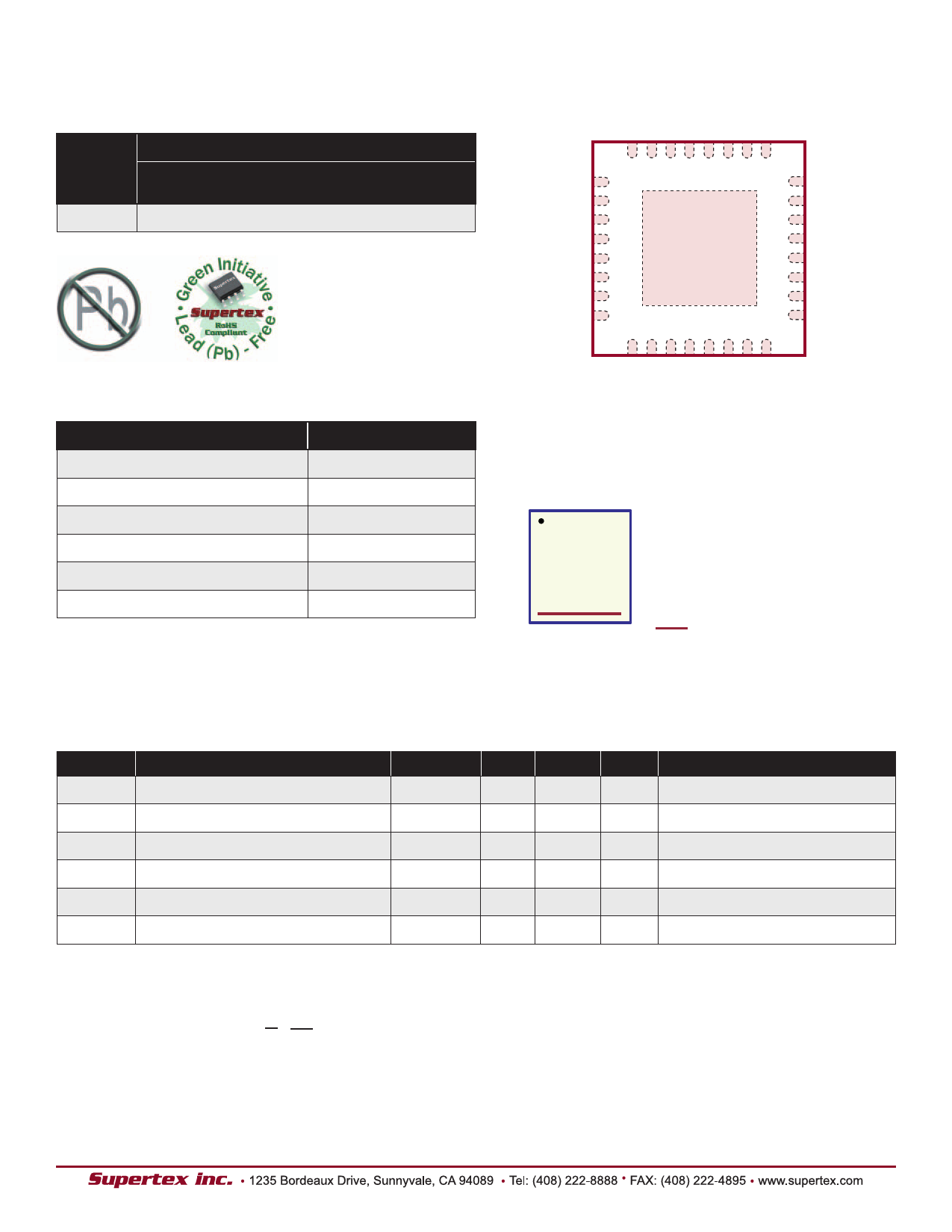
Pin Configuration
HV509
32
Absolute Maximum Ratings
Parameter
Value
Logic supply, VDD
High voltage supply, VPP
Translator supply voltage, VBIAS
Logic input levels
Operating junction temperature
-0.5V to 7.0V
215V
-0.5V to 7.0V
-0.5V to VDD + 0.5V
-40°C to +125°C
Storage temperature range
-65°C to +150°C
Absolute Maximum Ratings are those values beyond which damage to the
device may occur. Functional operation under these conditions is not implied.
Continuous operation of the device at the absolute rating level may affect
device reliability. All voltages are referenced to device ground.
1 32-Lead QFN
(top view)
Pads are at the bottom of the package.
Exposed heat slug is at VPP potential.
Product Marking
HV509
LLLLLL
YYWW
AAACCC
L = Lot Number
YY = Year Sealed
WW = Week Sealed
A = Assembler ID
C = Country of Origin
= “Green” Packaging
32-Lead QFN
Operating Supply Voltages and Conditions
Symbol Parameter
Min
Typ Max
VDD
VBIAS
VPP
V
IH
VIL
TA
Logic supply voltage
Level translator supply voltage
Positive high voltage supply
High-level input voltage
Low-level input voltage
Operating temperature
2.0
2.6
50
0.9V
DD
0
0
3.0 5.5
-
6.6
-
200
-
V
DD
-
0.1VDD
-
+70
Notes:
(1) External ground noise reduction circuit will be provided by design upon characterization.
(2) Power-up sequence should be the following*:
1. Apply ground
2. Apply VDD
3. Set all inputs (DIN, CLK, LE , POL) to a known state
4. Apply VBIAS
5. Apply VPP
(3) Power-down sequence should be the reverse of the above
Units
V
V
V
V
V
°C
Conditions
---
---
---
---
---
---
*This power up sequence requires an external high voltage diode between VDD and VPP. Without the diode, power up VPP to a VDD level first to
bias the silicon substrate. After all other signals are powered, finish raising the VPP to its final level.
2
Share Link: 