HV5308B データシートの表示(PDF) - Supertex Inc
部品番号
コンポーネント説明
メーカー
HV5308B Datasheet PDF : 12 Pages
| |||
HV5308B
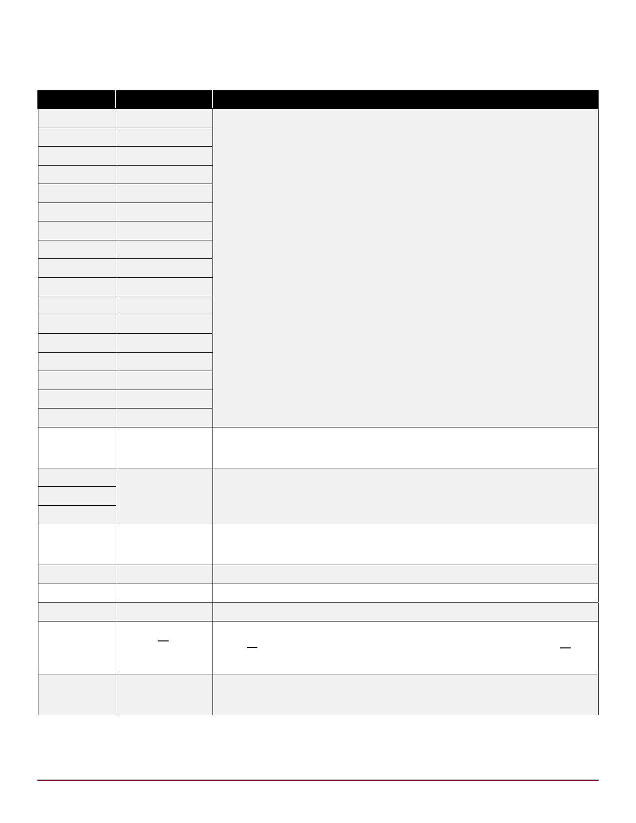
44-Lead Quad Cerpac/PLCC Pin Assignment (DJ/PJ)
Pin #
Function
Description
1
HVOUT17
2
HVOUT16
3
HVOUT15
4
HVOUT14
5
HVOUT13
6
HVOUT12
7
HVOUT11
8
HVOUT10
High voltage outputs.
9
HVOUT9
High voltage push-pull outputs, which, depending on controlling low voltage data,
10
HVOUT8
can drive loads either to GND, or to VPP rail levels.
11
HVOUT7
12
HVOUT6
13
HVOUT5
14
HVOUT4
15
HVOUT3
16
HVOUT2
17
HVOUT1
Serial data output.
18
DATA OUT
Data output for cascading to the data input of the next device.
19
20
N/C
No connect.
21
Data shift register clock
22
CLK
Input are shifted into the shift register on the positive edge of the clock.
23
GND
Logic and high voltage ground
24
VPP
High voltage power rail.
25
VDD
Low voltage logic power rail.
Latch enable input.
26
LE
When LE is HIGH, shift register data is transferred into a data latch. When LE is
LOW, data is latched, and new data can be clocked into the shift register.
Serial data input.
27
DATA IN
Data needs to be present before each rising edge of the clock.
Supertex inc. ● 1235 Bordeaux Drive, Sunnyvale, CA 94089 ● Tel: 408-222-8888 ● www.supertex.com
8
Share Link: 