HV574 データシートの表示(PDF) - Supertex Inc
部品番号
コンポーネント説明
メーカー
HV574 Datasheet PDF : 7 Pages
| |||
HV574
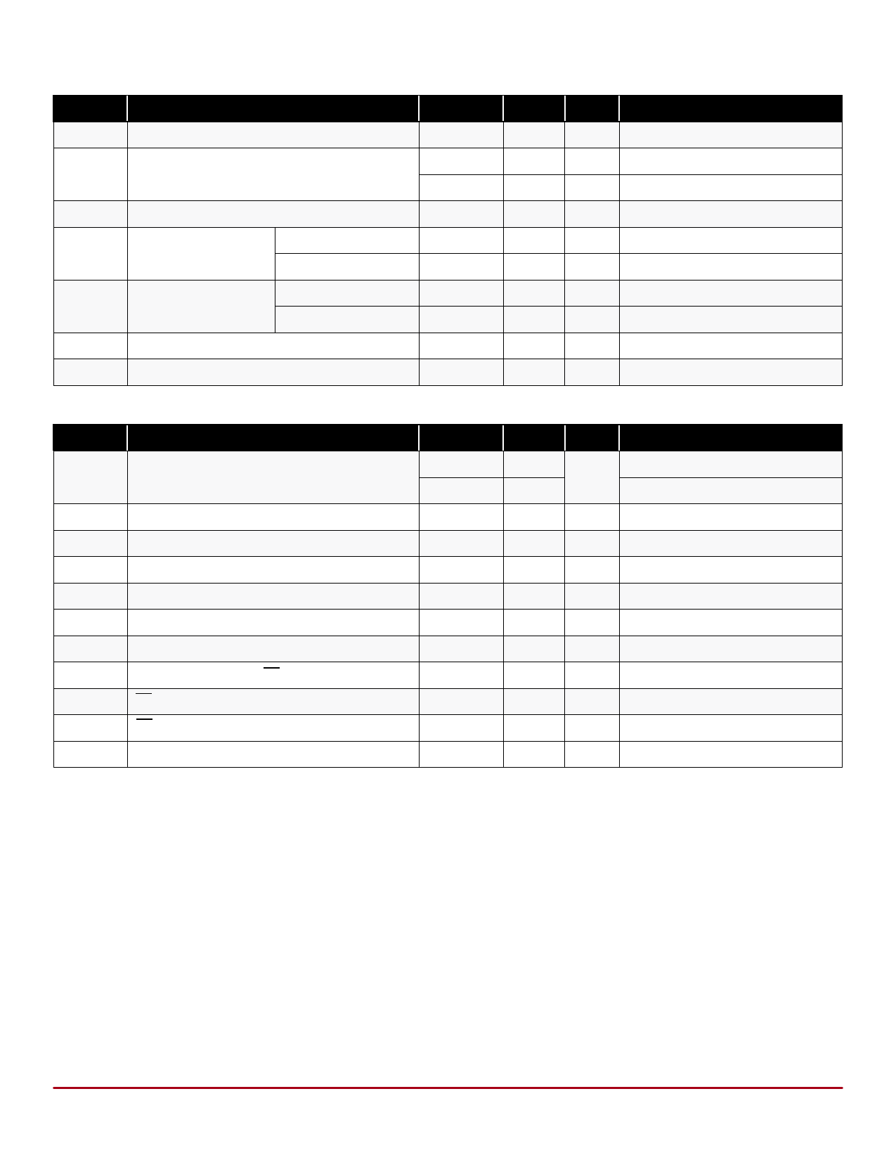
DC Electrical Characteristics (Over recommended operating conditions unless otherwise noted)
Sym Parameter
Min
Max Units Conditions
IDD
VDD supply current
IPP
Quiescent VPP supply current
-
30
mA VDD = VDD max, fCLK = 25MHz
-
100 µA Outputs high
-
100 µA Outputs low
IDDQ
Quiescent VDD supply current
VOH
High-level output
HVOUT
Data out
VOL
Low-level output
HVOUT
Data out
IIH
High-level logic input current
IIL
Low-level logic input current
-
VPP -9.0
VDD -0.5
-
-
-
-
100
-
-
3.75
0.5
1.0
-1.0
µA All VIN = VDD
V IO = -30mA, VPP = +80V
V IO = -100µA
V IO = +15mA, VDD = +5.0V
V IO = +100µA
µA VIH = VDD
µA VIL = 0V
AC Electrical Characteristics (TA = 85°C max. Logic signal inputs and data inputs have tr, tf ≤ 5.0ns [10% and 90% points])
Sym Parameter
Min
Max Units Conditions
fCLK
Clock frequency
0.001
0.001
25
MHz VDD = 4.5V, TJ = 25OC
20
VDD = 4.5V, TJ = 125OC
tWL, tWH Clock width high or low
20
-
ns ---
tSU
Data set-up time before clock rises
0
-
ns ---
tH
Data hold time after clock rises
15
-
ns ---
tON, tOFF Time from latch enable to HVOUT
-
500
ns CL = 15pF
tDHL
Delay time clock to data high to low
-
38
ns CL = 15pF, VDD = 5.0V
tDLH
Delay time clock to data low to high
-
38
ns CL = 15pF, VDD = 5.0V
tDLE* Delay time clock to LE low to high
25
-
ns ---
tWLE
LE pulse width
25
-
ns ---
tSLE
LE set-up time before clock rises
0
-
ns ---
tr, tf
Output rise/fall time
-
1.0
µs CL = 600pF, HVOUT from 0 - 60V
* tDLE is not required but is recommended to produce stable HV outputs and thus minimize power dissipation and current spikes (allows internal SR
output to stabilize).
Doc.# DSFP-HV574
A061913
Supertex inc.
3
www.supertex.com
Share Link: 