HV852(2006) データシートの表示(PDF) - Supertex Inc
部品番号
コンポーネント説明
メーカー
HV852 Datasheet PDF : 6 Pages
| |||
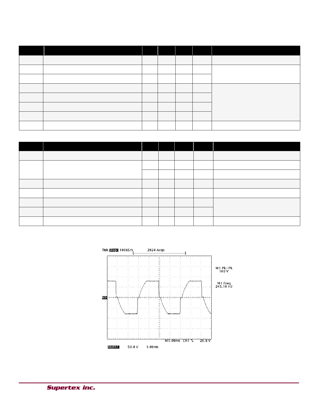
Typical Output Waveform
HV852
Test Conditions:
HV852 driving a 1.0in2 EL lamp
VDD= 3.6V and REL= 1.5MΩ,
VA-VB waveform
Functional Block Diagram
VDD
EN
CLKIN
CLKEN
REL
VDD
Capacitor
Charge
Pump Circuit
VSENSE
High
Voltage
VA
Level
Feedback
Trans-
lators
VDD
VB
EL
Oscillator
MOSFET
Full Bridge
GND
Pin Description
Name
VDD
R
EL
EN
CLKIN
CLKEN
Gnd
VB
VA
Description
Input supply voltage pin.
An external resistor to VDD will set the EL lamp frequency. When using an external clock to set the EL lamp frequency, the
REL pin should be connected to ground.
Enable input pin. Logic high will turn the device on. An external R-C circuit can be added for a delayed turn off.
Logic input pin. An external logic clock applied to this pad can be used to set the EL lamp frequency (see Figure 3). The
EL lamp frequency is the external clock frequency divided by 128. This is useful for applications requiring the EL lamp to
be synchronized to a system clock. Connect to ground when not in use.
Logic input pin. Logic high will cause the EL lamp frequency to be set by the CLKIN input. Logic low will cause the EL
lamp frequency to be set by the external REL resistor.
IC ground pin.
EL lamp driver output pin. The EL lamp is connected across VA and VB terminals.
EL lamp driver output pin. The EL lamp is connected across VA and VB terminals.
3
Share Link: 