HV9102P データシートの表示(PDF) - Supertex Inc
部品番号
コンポーネント説明
メーカー
HV9102P Datasheet PDF : 7 Pages
| |||
HV9100/HV9102/HV9103
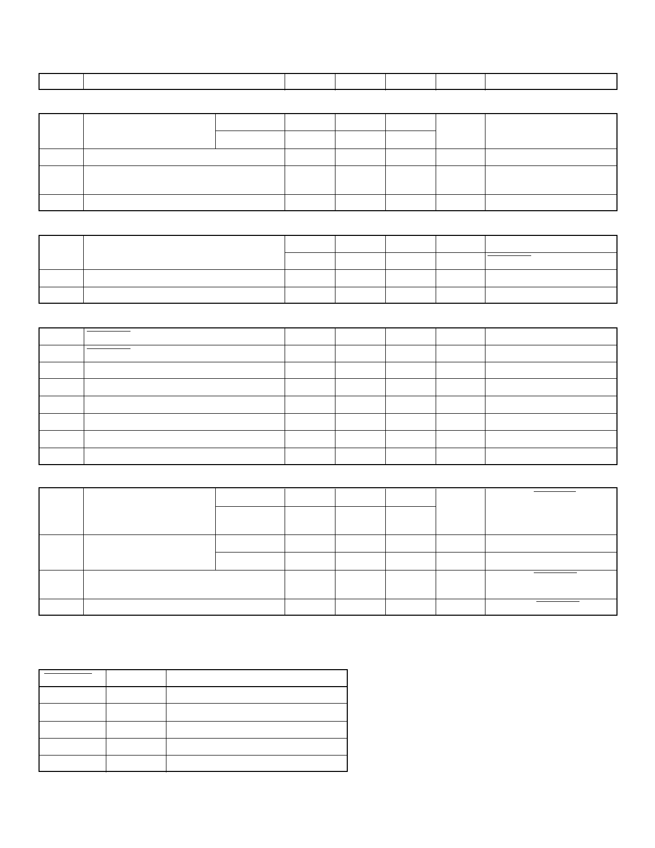
Electrical Characteristics (Continued)
(VDD = 10V, +VIN = 48V, Discharge = -VIN = 0V, RBIAS = 390KΩ, ROSC = 330KΩ,TA = 25°C, unless otherwise specified)
Symbol Parameters
Min
Typ
Max
Unit Conditions
Pre-Regulator/Startup
+VIN Allowable Input Voltage
HV9100
HV9102/03
70
V
IIN = 10µA
120
VTH
VLOCK
Input Leakage Current
VDD Pre-regulator Turn-off
Threshold Voltage
Undervoltage Lockout
10
µA
VDD > 9.4V
7.8
8.6
9.4
V
IPREREG = 10µA
7.0
8.1
8.9
V
RL = 100Ω from Drain to VDD
Supply
IDD
Supply Current
IBIAS
Bias Current
VDD
Operating Range
0.60
1.0
mA
0.55
20
mA Shutdown = -VIN
µA
9.0
13.5
V
Logic
tSD
Shutdown Delay Time1
tSW
Shutdown Pulse Width1
tRW
RESET Pulse Width1
tLW
Latching Pulse Width1
VIL
Input Low Voltage
VIH
Input High Voltage
IIH
Input High Current
IIL
Input Low Current
50
100
ns
VSOURCE = -VIN
50
ns
50
ns
25
ns
2.0
V
7.0
V
1.0
5.0
µA
VIN = 10V
-25
-35
µA
VIN = 0V
MOSFET Switch
BVDSS Breakdown Voltage
RDS(ON) Drain-to-Source
On-resistance
HV9100
150
V
VSOURCE = Shutdown = 0V,
HV9102/03
200
ID = 100µA,
TA = -55°C to 125°C
HV9100
3.5
5.0
Ω
VSOURCE = 0V, ID = 100mA
HV9102/03
7.0
Ω
IDSS
OFF State Drain Leakage Current
CDS
Drain Capacitance
Note:
1. Guaranteed by design. Not subject to production test.
10
µA
VSOURCE = Shutdown = 0V,
VDRAIN = 100V
35
pF
VDS = 25V, Shutdown = 0V
Truth Table
Shutdown
Reset
H
H
H
H→L
L
H
L
L
L→H
L
Output
Normal Operation
Normal Operation, No Change
Off, Not Latched
Off, Latched
Off, Latched, No Change
3
Share Link: 