ICS81006I データシートの表示(PDF) - Integrated Device Technology
部品番号
コンポーネント説明
メーカー
ICS81006I Datasheet PDF : 14 Pages
| |||
ICS81006I
VCXO-TO-6 LVCMOS OUTPUTS
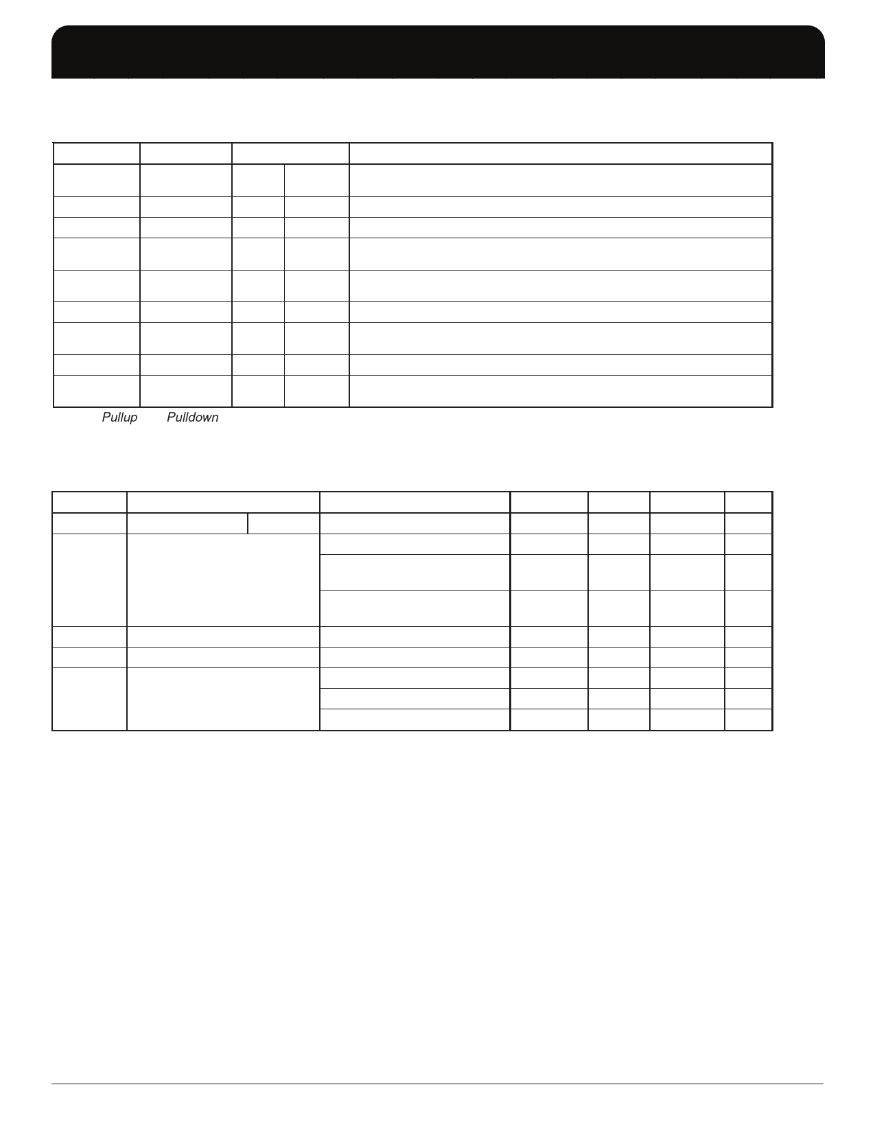
TABLE 1. PIN DESCRIPTIONS
Number
Name
Type
Description
1, 2
XTAL_IN,
XTAL_OUT
Input
Crystal oscillator interface. XTAL_IN is the input.
XTAL_OUT is the output.
3
VDD
Power
4
VC
Input
Core supply pin.
Control voltage input.
5
DIV_SEL_Q5
Input
Pulldown
Output divider select pin for Q5 output. When LOW, ÷1. When HIGH,
÷2, LVCMOS/LVTTL interface levels.
6
OE1
Input
Pullup
Output enable pin. When HIGH, Q5 output is enabled.
When LOW, forces Q5 to HiZ state. LVCMOS/LVTTL interface levels.
7, 11, 15, 19
GND
Power
Power supply ground.
8, 10, 12,
14, 16, 18
Q5, Q4, Q3,
Q2, Q1, Q0
Output
Single-ended clock outputs. LVCMOS/LVTTL interface levels.
15Ω typical output impedance.
9, 13, 17
20
VDDO
OE0
Power
Input
Pullup
Output supply pins.
Output enable pin. When HIGH, Q0:Q4 outputs are enabled. When
LOW, forces Q0:Q4 to HiZ state. LVCMOS/LVTTL interface levels.
NOTE: Pullup and Pulldown refers to internal input resistors. See Table 2, Pin Characteristics, for typical values.
TABLE 2. PIN CHARACTERISTICS
Symbol
CIN
Parameter
Input Capacitance OE0, OE1
CPD
Power Dissipation Capacitance
R
PULLUP
RPULLDOWN
Input Pullup Resistor
Input Pulldown Resistor
ROUT
Output Impedance
Test Conditions
VDD = VDDO = 3.465V
VDD = 3.465V or 2.625V,
VDDO = 2.625V
VDD = 3.465V or 2.625V,
VDDO = 2V
VDDO = 3.3V
VDDO = 2.5V
VDDO = 1.8V
Minimum
Typical
4
Maximum
3
Units
pF
pF
4
pF
6
pF
51
kΩ
51
kΩ
20
Ω
25
Ω
38
Ω
IDT™ / ICS™ VCXO-TO-LVCMOS OUTPUTS
2
ICS81006AKI REV A OCTOBER 2, 2006
Share Link: 