ICS81006I データシートの表示(PDF) - Integrated Device Technology
部品番号
コンポーネント説明
メーカー
ICS81006I Datasheet PDF : 14 Pages
| |||
ICS81006I
VCXO-TO-6 LVCMOS OUTPUTS
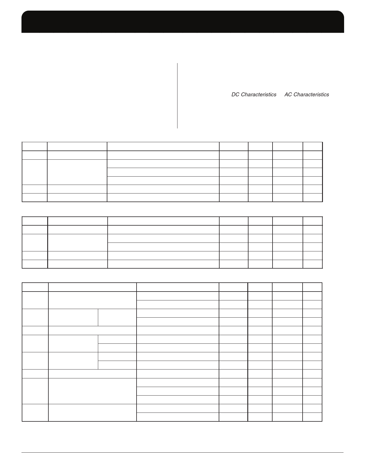
ABSOLUTE MAXIMUM RATINGS
Supply Voltage, VDD
4.6V
Inputs, VI
-0.5V to VDD + 0.5 V
Outputs, VO
-0.5V to VDD + 0.5V
Package Thermal Impedance, θJA 60.4°C/W (0 mps)
Storage Temperature, TSTG
-65°C to 150°C
NOTE: Stresses beyond those listed under Absolute
Maximum Ratings may cause permanent damage to the
device. These ratings are stress specifications only. Functional op-
eration of product at these conditions or any conditions beyond
those listed in the DC Characteristics or AC Characteristics is not
implied. Exposure to absolute maximum rating conditions for ex-
tended periods may affect product reliability.
TABLE 3A. POWER SUPPLY DC CHARACTERISTICS, VDD = 3.3V±5%, VDDO = 3.3V±5% = 2.5V±5% = 1.8V±0.2V, TA = -40°C TO 85°C
Symbol Parameter
Test Conditions
Minimum Typical Maximum Units
VDD
Core Supply Voltage
3.135
3.3
3.465
V
3.135
3.3
3.465
V
VDDO
Output Supply Voltage
2.375
2.5
2.625
V
1.6
1.8
2.0
V
IDD
Power Supply Current
IDDO
Output Supply Current
50
mA
20
mA
TABLE 3B. POWER SUPPLY DC CHARACTERISTICS, VDD = 2.5V±5%, VDDO = 2.5V±5% = 1.8V±0.2V, TA = -40°C TO 85°C
Symbol Parameter
Test Conditions
Minimum Typical Maximum
VDD
VDDO
Core Supply Voltage
Output Supply Voltage
2.375
2.5
2.625
2.375
2.5
2.625
1.6
1.8
2.0
IDD
Power Supply Current
50
IDDO
Output Supply Current
20
Units
V
V
V
mA
mA
TABLE 3C. LVCMOS/LVTTL DC CHARACTERISTICS, TA = -40°C TO 85°C
Symbol Parameter
Test Conditions
Minimum Typical Maximum Units
VIH
Input High Voltage
VDD = 3.3V ± 5%
2
VDD = 2.5V ± 5%
1.7
VDD + 0.3
V
VDD + 0.3
V
VIL
Input Low Voltage
OE0, OE1,
DIV_SEL_Q5
VDD = 3.3V ± 5%
VDD = 2.5V ± 5%
-0.3
-0.3
0.8
V
0.7
V
VC
VCXO Control Voltage
0
VDD
V
IIH
DIV_SEL_Q5
Input High Current
OE0, OE1
VDD = 3.3V or 2.5V ± 5%
V = 3.3V or 2.5V ± 5%
DD
150
µA
5
µA
IIL
DIV_SEL_Q5
Input Low Current
OE0, OE1
VDD = 3.3V or 2.5V ± 5%
VDD = 3.3V or 2.5V ± 5%
-5
-150
µA
µA
II
Input Current of VC pin
VDD = 3.465V or 2.625V
-100
100
µA
VDDO = 3.3V ± 5%
2.6
V
VOH
Output High Voltage;NOTE 1
V
DDO
=
2.5V
±
5%
1.8
V
VDDO = 1.8V ± 0.2V
1.5
V
VOL
Output Low Voltage;NOTE 1
VDDO = 3.3V or 2.5V ± 5%
VDDO = 1.8V ± 0.2V
0.5
V
0.4
V
NOTE 1: Outputs terminated with 50Ω to VDDO/2. See Parameter Measurement section, "Load Test Circuit" diagrams.
IDT™ / ICS™ VCXO-TO-LVCMOS OUTPUTS
3
ICS81006AKI REV A OCTOBER 2, 2006
Share Link: 