AV9248F-61 データシートの表示(PDF) - Integrated Circuit Systems
部品番号
コンポーネント説明
メーカー
AV9248F-61 Datasheet PDF : 9 Pages
| |||
ICS9248-61
Absolute Maximum Ratings
Supply Voltage . . . . . . . . . . . . . . . . . . . . . . . . . . . 7.0V
Logic Inputs . . . . . . . . . . . . . . . . . . . . . . . . . . . . GND 0.5 V to VDD +0.5 V
Ambient Operating Temperature . . . . . . . . . . . . 0°C to +70°C
Storage Temperature . . . . . . . . . . . . . . . . . . . . . . 65°C to +150°C
Stresses above those listed under Absolute Maximum Ratings may cause permanent damage to the device. These ratings are
stress specifications only and functional operation of the device at these or any other conditions above those listed in the
operational sections of the specifications is not implied. Exposure to absolute maximum rating conditions for extended periods
may affect product reliability.
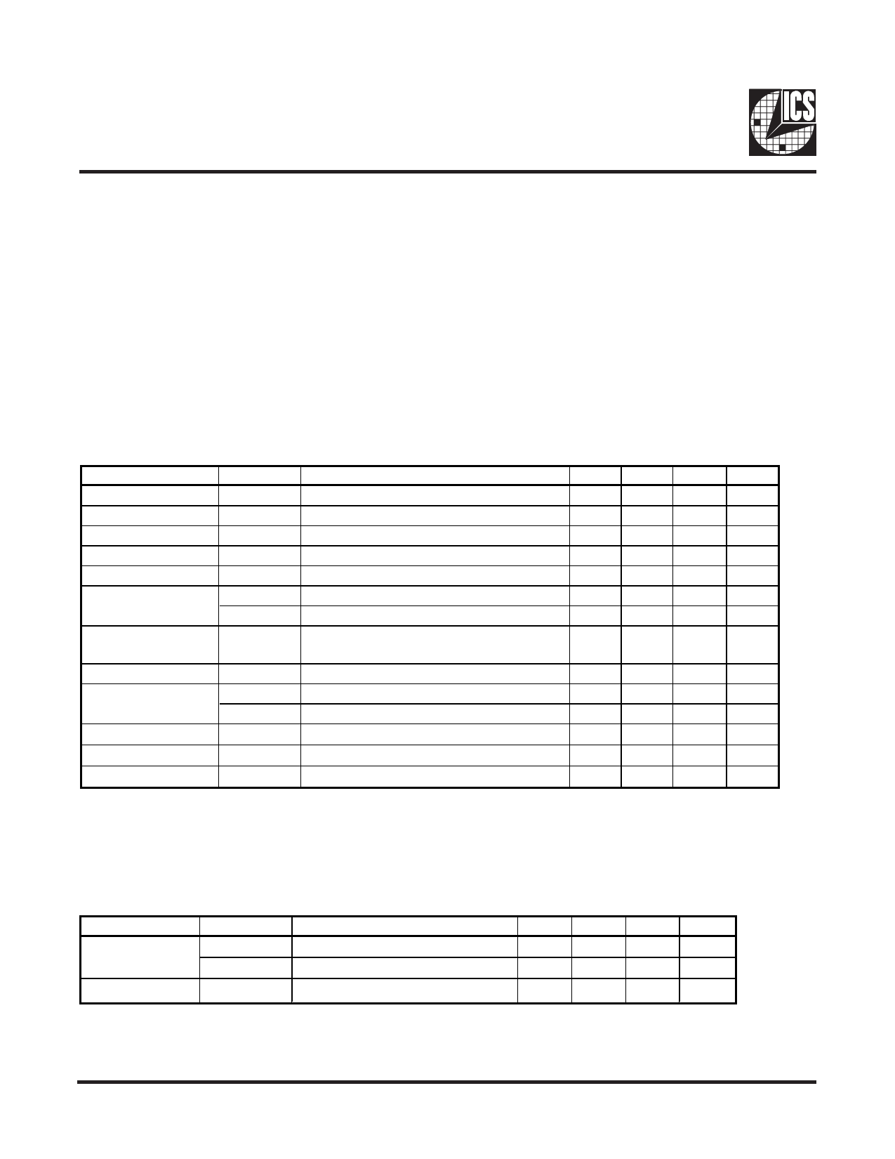
Electrical Characteristics - Input/Supply/Common Output Parameters
TA = 0 - 70C; Supply Voltage VDD = VDDL = 3.3 V +/-5% (unless otherwise stated)
PARAMETER
SYM B OL
CONDITIONS
MIN TYP MAX UNITS
Input High Voltage
VIH
Input Low Voltage
VIL
Input High Current
IIH
VIN = VDD
Input Low Current
IIL1
VIN = 0 V; Inputs with no pull-up resistors
Input Low Current
IIL2
VIN = 0 V; Inputs with pull-up resistors
Operating
IDD3.3OP66 CL = 0 pF; Select @ 66MHz
Supply Current
IDD3.3OP100 CL = 0 pF; Select @ 100MHz
Power Down Supply
Current
IDD3 .3 PD
CL = 0 pF;
With input address to Vdd or GND
Input frequency
Fi
VDD = 3.3 V;
Input Capacitance1
Transition Time1
Clk Stabilization1
Skew1
CIN
CINX
Ttrans
TSTAB
TCPU-PCI1
Logic Inputs
X1 & X2 pins
To 1st crossing of target Freq.
From VDD = 3.3 V to 1% target Freq.
VT = 1.5 V;
1Guaranteed by design, not 100% tested in production.
2
VDD+0.3 V
VSS-0.3
0.8
V
0.1
5
µA
-5
2.0
µA
-200 -100
µA
60 180 mA
66 180 mA
70 600
11 14.318 16
5
27
36
45
3
3
1.5 2.4
4
µA
M Hz
pF
pF
ms
ms
ns
Electrical Characteristics - Input/Supply/Common Output Parameters
TA = 0 - 70C; Supply Voltage VDD = 3.3 V+/-5%, VDDL = 2.5 V+/-5% (unless otherwise stated)
PARAMETER
SYMBOL
CONDITIONS
MIN TYP MAX UNITS
Operating
IDD2.5OP66 CL = 0 pF; Select @ 66.8 MHz
16
72
mA
Supply Current
Skew1
IDD2.5OP100 CL = 0 pF; Select @ 100 MHz
tCPU-PCI2 VT = 1.5 V; VTL = 1.25 V
23
100
mA
1.5
3
4
ns
1Guaranteed by design, not 100% tested in production.
6
Share Link: 