ICS93732 データシートの表示(PDF) - Integrated Circuit Systems
部品番号
コンポーネント説明
メーカー
ICS93732 Datasheet PDF : 8 Pages
| |||
ICS9373 2
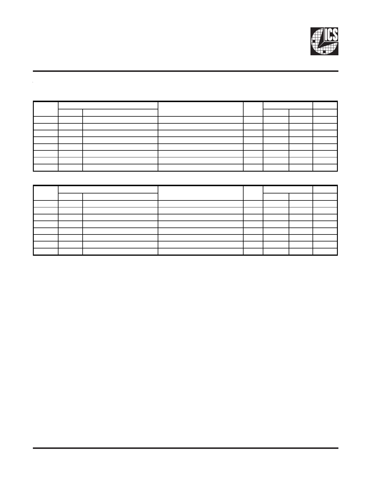
Bytes 0 to 4 are reseved power up default = 1. This allows operation with main clock.
BYTE
Affected Pin
5
Pin #
Name
Bit 7
2, 1
DDR0(T&C)
Bit 6
4, 5
DDR1(T&C)
Bit 5
-
-
Bit 4
-
-
Bit 3 13, 14
DDR2(T&C)
Bit 2 17, 16
DDR3(T&C)
Bit 1
-
-
Bit 0
-
-
Note: PWD = Power Up Default
BYTE
Affected Pin
6
Pin #
Name
Bit 7
-
-
Bit 6
-
-
Bit 5
-
-
Bit 4
-
-
Bit 3 24, 25
DDR4(T&C)
Bit 2
-
-
Bit 1 26, 27
DDR5(T&C)
Bit 0
-
-
Note: PWD = Power Up Default
Control Function
Output Control
Output Control
Reserved
Reserved
Output Control
Output Control
Reserved
Reserved
Control Function
Reserved
Reserved
Reserved
Reserved
Output Control
Reserved
Output Control
Reserved
Type
RW
RW
X
X
RW
RW
X
X
Bit Control
0
1
DISABLE ENABLE
DISABLE ENABLE
-
-
-
-
DISABLE ENABLE
DISABLE ENABLE
-
-
-
-
PWD
1
1
1
1
1
1
1
1
Type
X
X
X
X
RW
X
RW
X
Bit Control
0
1
-
-
-
-
-
-
-
-
DISABLE ENABLE
-
-
DISABLE ENABLE
-
-
PWD
0
0
0
1
1
1
1
1
0578H—02/19/04
6
Share Link: 