ICX285 データシートの表示(PDF) - Sony Semiconductor
部品番号
コンポーネント説明
メーカー
ICX285
Sony Semiconductor

ICX285 Datasheet PDF : 24 Pages
| |||
ICX285AQ
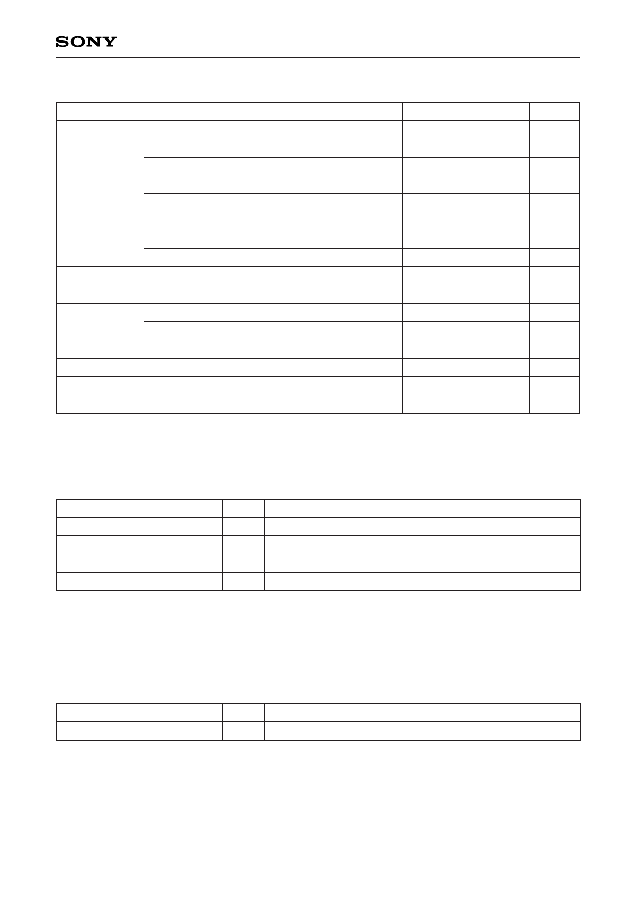
Absolute Maximum Ratings
Against φSUB
Against φGND
Against φVL
Between input
clock pins
Item
VDD, VOUT, φRG – φSUB
Vφ2A, Vφ2B – φSUB
Vφ1, Vφ3, Vφ4, VL – φSUB
Hφ1, Hφ2, GND – φSUB
CSUB – φSUB
VDD, VOUT, φRG, CSUB – GND
Vφ1, Vφ2A, Vφ2B, Vφ3, Vφ4 – GND
Hφ1, Hφ2 – GND
Vφ2A, Vφ2B – VL
Vφ1, Vφ3, Vφ4, Hφ1, Hφ2, GND – VL
Voltage difference between vertical clock input pins
Hφ1 – Hφ2
Hφ1, Hφ2 – Vφ4
Storage temperature
Guaranteed temperature of performance
Operating temperature
∗1 +24V (Max.) when clock width < 10µs, clock duty factor < 0.1%.
+16V (Max.) is guaranteed for turning on or off power supply.
Ratings
–40 to +12
–50 to +15
–50 to +0.3
–40 to +0.3
–25 to
–0.3 to +22
–10 to +18
–10 to +6.5
–0.3 to +28
–0.3 to +15
to +15
–6.5 to +6.5
–10 to +16
–30 to +80
–10 to +60
–10 to +75
Unit Remarks
V
V
V
V
V
V
V
V
V
V
V
∗1
V
V
°C
°C
°C
Bias Conditions
Item
Symbol
Min.
Typ.
Max.
Unit Remarks
Supply voltage
Protective transistor bias
Substrate clock
Reset gate clock
VDD
VL
φSUB
φRG
14.55
15.0
∗2
∗3
∗3
15.45
V
∗2 VL setting is the VVL voltage of the vertical clock waveform, or the same voltage as the VL power supply for
the V driver should be used.
∗3 Do not apply a DC bias to the substrate clock and reset gate clock pins, because a DC bias is generated
within the CCD.
DC Characteristics
Item
Supply current
Symbol
IDD
Min.
Typ.
Max.
Unit Remarks
9
11
mA
–4–
Share Link: