ICX084 データシートの表示(PDF) - Sony Semiconductor
部品番号
コンポーネント説明
メーカー
ICX084
Sony Semiconductor

ICX084 Datasheet PDF : 18 Pages
| |||
ICX084AK
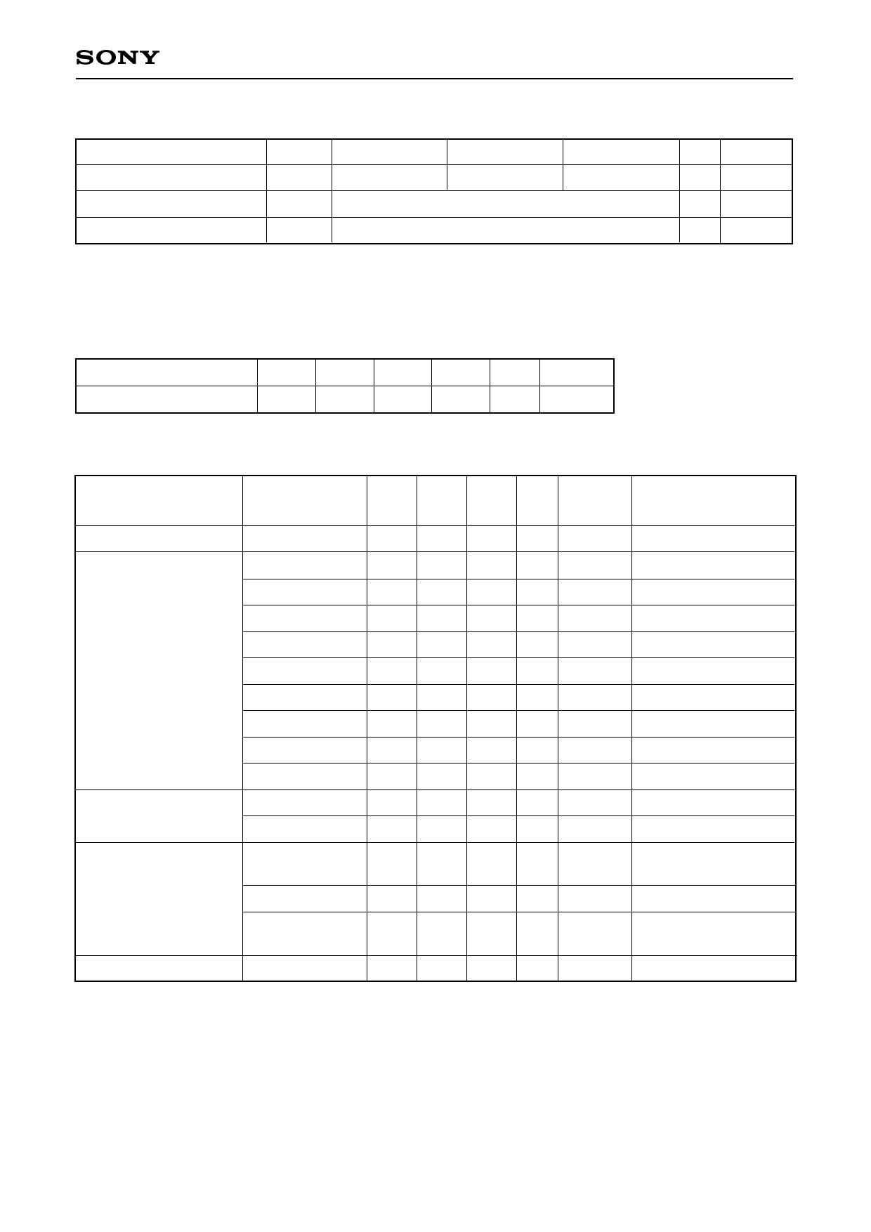
Bias Conditions
Item
Symbol
Min.
Typ.
Max.
Unit Remarks
Supply voltage
Protective transistor bias
Substrate clock
VDD
VL
φSUB
14.55
15.0
∗1
∗2
15.45
V
∗1 VL setting is the VVL voltage of the vertical transfer clock waveform, or the same power supply as the VL
power supply for the V driver should be used.
∗2 Set SUBCIR pin to open when applying a DC bias to the substrate clock pin.
DC Characteristics
Item
Supply current
Symbol Min. Typ. Max. Unit Remarks
IDD
6
8
mA
Clock Voltage Conditions
Waveform
Item
Symbol
Min. Typ. Max. Unit diagram
Remarks
Readout clock voltage VVT
14.55 15.0 15.45 V
VVH02
–0.05 0 0.05 V
VVH1, VVH2, VVH3 –0.2 0 0.05 V
VVL1, VVL2, VVL3 –8.0 –7.5 –7.0 V
Vertical transfer clock
voltage
Vφ1, Vφ2, Vφ3
I VVL1 – VVL3 I
6.8 7.5 8.05 V
0.1 V
VVHH
1.0 V
VVHL
2.3 V
VVLH
1.0 V
VVLL
1.0 V
Horizontal transfer
VφH
clock voltage
VHL
4.75 5.0 5.25 V
–0.05 0 0.05 V
1
2
VVH = VVH02
2
2
VVL = (VVL1 + VVL3)/2
2
2
2
High-level coupling
2
High-level coupling
2
Low-level coupling
2
Low-level coupling
3
3
Reset gate clock
voltage
VφRG
VRGLH – VRGLL
VRGH
4.5 5.0 5.5 V
0.8 V
VDD VDD VDD
+0.4 +0.6 +0.8 V
4
Input through 0.01µF
capacitance
4
Low-level coupling
4
Substrate clock voltage VφSUB
21.5 22.5 23.5 V
5
–3–
Share Link: