IDT49C460 データシートの表示(PDF) - Integrated Device Technology
部品番号
コンポーネント説明
メーカー
IDT49C460 Datasheet PDF : 32 Pages
| |||
IDT49C460/A/B/C/D/E
32-BIT CMOS ERROR DETECTION AND CORRECTION UNIT
MILITARY AND COMMERCIAL TEMPERATURE RANGES
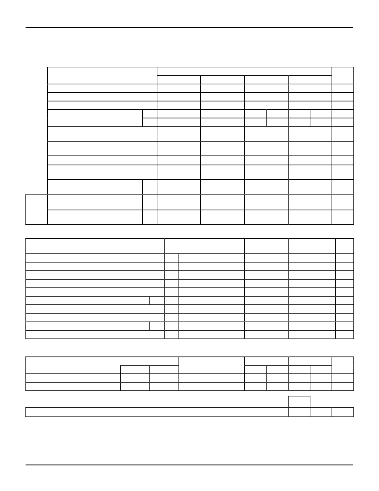
IDT49C460B AC ELECTRICAL CHARACTERISTICS
(Guaranteed Military Range Performance) Temperature range: –55°C to +125°C, VCC = 5.0V ± 10%
The inputs switch between 0V to 3V with signal measured at the 1.5V level.
PROPAGATION DELAYS(1)
From Input
SC0–7
To Output
DATA0–31
ERROR
MULT ERROR Unit
DATA0–31 (3)
28
33(2)
28
30
ns
CB0–7 (CODE ID1,0 = 00, 11)
17
33
20
23
ns
CB0–7 (CODE ID1,0 = 10)
LEOUT/GENERATE
19
u
—
d
24
23
—
—
ns
15
d
26
d
26
ns
—
u
26
u
26
ns
CORRECT
Not Internal Control Mode
—
26
—
—
ns
DIAG MODE
Not Internal Control Mode
20
29
23
27
ns
CODE ID1,0
21
29
24
29
ns
LEIN
30
41
33
From latched to Transparent
LEDIAG
u
18
32
22
From latched to Transparent
Internal LEDIAG
u
19
35
22
Control From latched to Transparent
Mode DATA0–31
u
19
35(2)
23
Via Diagnostic Latch
SET-UP AND HOLD TIMES RELATIVE TO LATCH ENABLES
36
ns
25
ns
27
ns
28
ns
2584 tbl 48
From Input
DATA0–31 (4)
CB0–7 (4)
DATA0–31(4, 6)
CB0–7 (CODE ID 00, 11)(4, 6)
CB0–7 (CODE ID 10)(4, 6)
CORRECT(4, 6)
DIAG MODE(4, 6)
CODE ID1,0(4, 6)
LEIN(4, 6)
DATA0–31(4, 6)
To Input
(Latching Data)
d
d
d
d
d
ud
d
d
ud
LEIN
LEIN
LEOUT/GENERATE
LEOUT/GENERATE
LEOUT/GENERATE
LEOUT/GENERATE
LEOUT/GENERATE
LEOUT/GENERATE
LEOUT/GENERATE
LEDIAG
OUTPUT ENABLE/DISABLE TIMES(5)
Set-up Time
Min.
4
4
23
18
18
14
20
20
23
4
Hold Time
Min.
4
4
0
0
0
0
0
0
0
3
Unit
ns
ns
ns
ns
ns
ns
ns
ns
ns
ns
2584 tbl 49
Enable
Disable
From Input
OE Byte0–3
OESC
Enable
d
d
Disable
u
u
MINIMUM PULSE WIDTHS
ud LEIN, LEOUT/GENERATE, LEDIAG
(Positive–going pulse)
To Output
DATA0–31
SC0–7
Min.
0
0
Max.
12
12
Min.
0
0
Min.
12
Max.
14
14
Unit
ns
ns
2584 tbl 50
ns
NOTES:
2584 tbl 51
1. CI = 50pF.
2. These parameters are combinational propagation delay calculations, and are not tested in production.
3. Data In or Correct Data Out measurement requires timing as shown in the Switching Waveforms.
4. Set-up and Hold times relative to Latch Enables (Latching Data).
5. Output tests specified with CI = 5pF and measured to 0.5V change of output level. Testing is performed at CI = 50pF and correlated to CI = 5pF.
6. Not production tested, guaranteed by characterization.
11.6
24
Share Link: 