IDT7130SA100JI データシートの表示(PDF) - Integrated Device Technology
部品番号
コンポーネント説明
メーカー
IDT7130SA100JI Datasheet PDF : 19 Pages
| |||
IDT7130SA/LA and IDT7140SA/LA
High-Speed 1K x 8 Dual-Port Static SRAM
Military, Industrial and Commercial Temperature Ranges
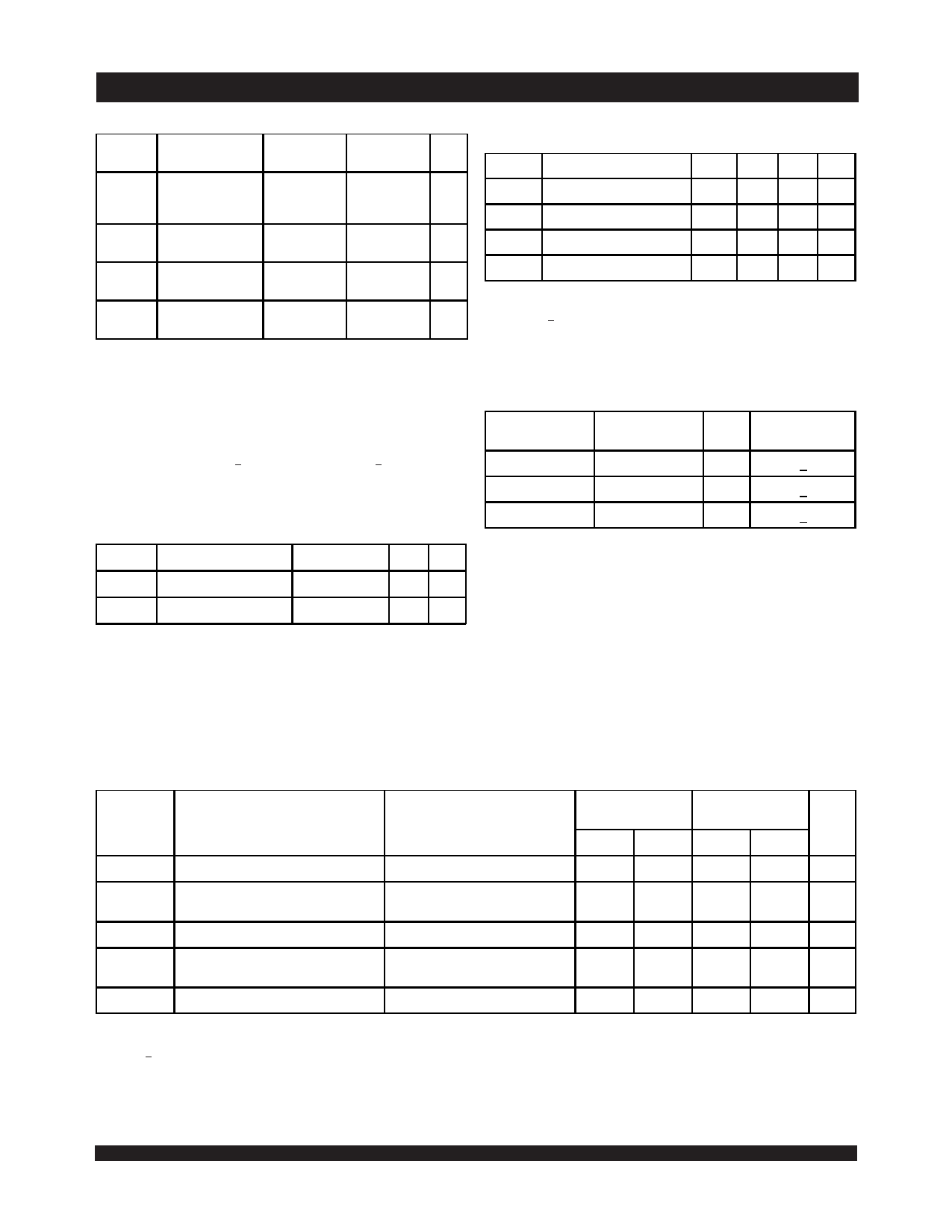
Absolute Maximum Ratings(1)
Symbol
Rating
Commercial
& Industrial
Military
Unit
VTERM(2)
Terminal Voltage
with Respect
to GND
-0.5 to +7.0 -0.5 to +7.0 V
TBIAS
Temperature
Under Bias
-55 to +125 -65 to +135 oC
TSTG
Storage
Temperature
-65 to +150 -65 to +150 oC
IOUT
DC Output
Current
50
50
mA
NOTES:
2689 tbl 01
1. Stresses greater than those listed under ABSOLUTE MAXIMUM RATINGS may
cause permanent damage to the device. This is a stress rating only and functional
operation of the device at these or any other conditions above those indicated in
the operational sections of the specification is not implied. Exposure to absolute
maximum rating conditions for extended periods may affect reliability.
2. VTERM must not exceed Vcc + 10% for more than 25% of the cycle time or 10ns
maximum, and is limited to < 20mA for the period of VTERM > Vcc + 10%.
Recommended DC Operating
Conditions
Symbol
Parameter
Min. Typ. Max. Unit
VCC Supply Voltage
4.5 5.0 5.5 V
GND Ground
VIH Input High Voltage
VIL Input Low Voltage
0
0
0V
2.2
____
6.0(2)
V
-0.5(1)
____
0.8
V
NOTES:
1. VIL (min.) > -1.5V for pulse width less than 10ns.
2. VTERM must not exceed Vcc + 10%.
2689 tbl 02
Recommended Operating
Temperature and Supply Voltage(1)
Grade
Ambient
GND
Vcc
Temperature
Military
-55OC to +125OC
0V
5.0V + 10%
Capacitance (TA = +25°C, f = 1.0MHz)
STQFP and TQFP Packages Only
Symbol
Parameter(1)
Conditions Max. Unit
CIN Input Capacitance
VIN = 3dV
9 pF
Commercial
0OC to +70OC
0V
5.0V + 10%
Industrial
-40OC to +85OC
0V
5.0V + 10%
NOTES:
2689 tbl 03
1. This is the parameter TA. This is the "instant on" case temperature.
COUT Output Capacitance
VOUT = 3dV
10 pF
NOTES:
2689 tbl 05
1. This parameter is determined by device characterization but is not production
tested.
2. 3dV references the interpolated capacitance when the input and output signals
switch from 0V to 3V or from 3V to 0V.
DC Electrical Characteristics Over the Operating
Temperature and Supply Voltage Range (VCC = 5.0V ± 10%)
7130SA
7140SA
Symbol
Parameter
Test Conditions
Min.
Max.
|ILI|
Input Leakage Current(1)
VCC = 5.5V, VIN = 0V to VCC
___
10
|ILO|
Output Leakage Current(1)
VCC - 5.5V,
CE = VIH, VOUT = 0V to VCC
___
10
VOL
Output Low Voltage (I/O0-I/O7)
IOL = 4mA
___
0.4
VOL
Open Drain Output
Low Voltage (BUSY, INT)
IOL = 16mA
___
0.5
VOH
Output High Voltage
IOH = -4mA
2.4
___
NOTE:
1. At Vcc < 2.0V leakages are undefined.
7130LA
7140LA
Min.
Max. Unit
___
5
µA
___
5
µA
___
0.4
V
___
0.5
V
2.4
___
V
2689 tbl 04
4
Share Link: 