IDT71V124S15 データシートの表示(PDF) - Integrated Device Technology
部品番号
コンポーネント説明
メーカー
IDT71V124S15
Integrated Device Technology

IDT71V124S15 Datasheet PDF : 8 Pages
| |||
IDT71V124, 3.3V CMOS Static RAM
1 Meg (128K x 8-Bit), Revolutionary Pinout
Commercial and Industrial Temperature Ranges
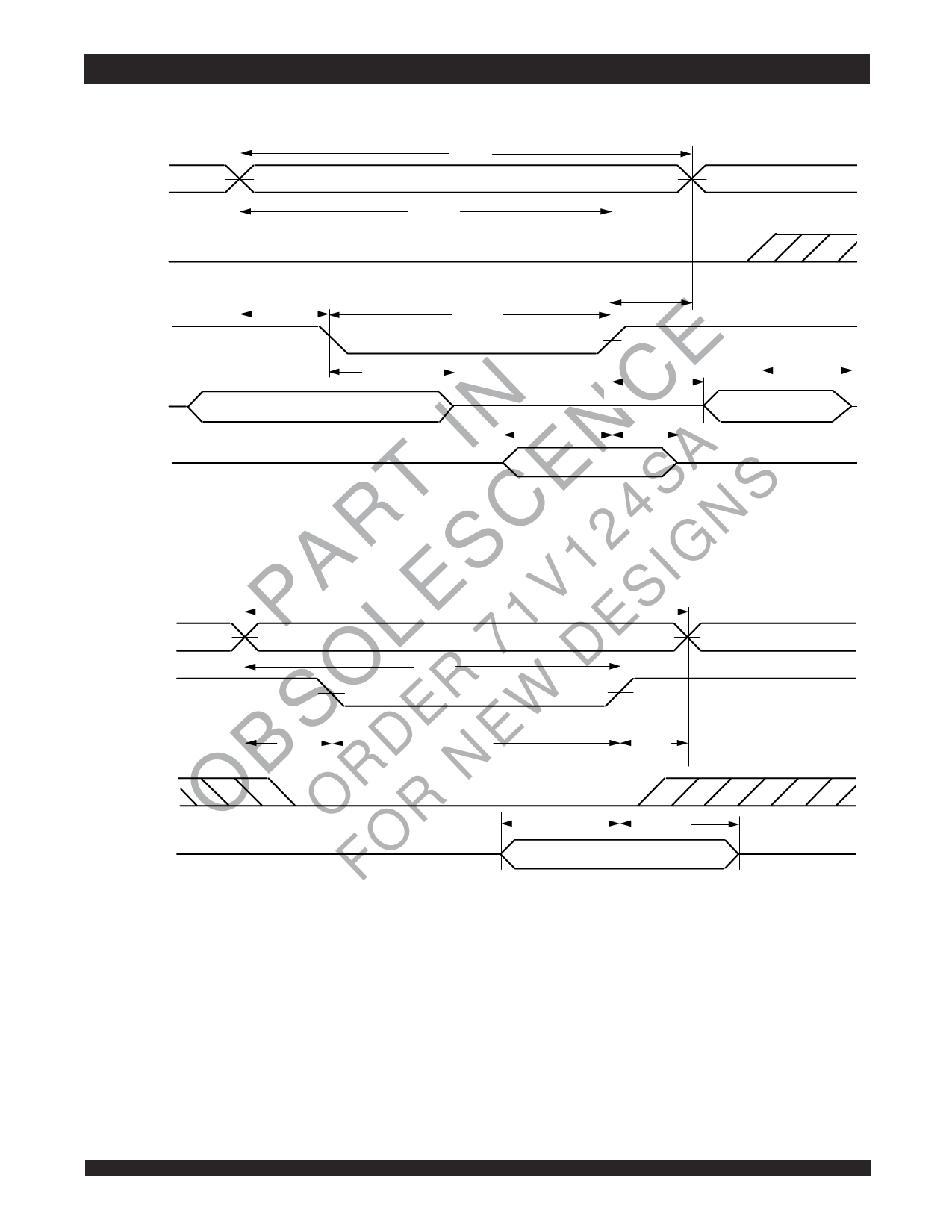
Timing Waveform of Write Cycle No.1 (WE Controlled Timing)(1,2,4)
ADDRESS
tWC
tAW
CS
tWR
WE
N CE DATAOUT
I N A DATAIN
tAS
(3)
tWHZ (5)
tWP (2)
tOW (5)
HIGH IMPEDANCE
tDH
tDW
DATAIN VALID
tCHZ (5)
(3)
3484 drw 07
ART SCE124SIGNS Timing Waveform of Write Cycle No. 2 (CS Controlled Timing)(1,4)
P LE 1V ES ADDRESS
O 7 D CS
tWC
tAW
S ER W tAS
tCW
tWR(3)
B RD NE WE
O OFOR DATAIN
tDW
tDH
DATAIN VALID
3484 drw 08
NOTES:
1. A write occurs during the overlap of a LOW CS and a LOW WE.
2. OE is continuously HIGH. During a WE controlled write cycle with OE LOW, tWP must be greater than or equal to tWHZ + tDW to allow the I/O drivers to turn off and data to be
placed on the bus for the required tDW. If OE is HIGH during a WE controlled write cycle, this requirement does not apply and the minimum write pulse is the specified tWP.
3. During this period, I/O pins are in the output state, and input signals must not be applied.
4. If the CS LOW transition occurs simultaneously with or after the WE LOW transition, the outputs remain in a high impedance state. CS must be active during the tCW write
period.
5. Transition is measured ±200mV from steady state.
6.642
Share Link: