IDT72421L12(1995) データシートの表示(PDF) - Integrated Device Technology
部品番号
コンポーネント説明
メーカー
IDT72421L12
(Rev.:1995)
(Rev.:1995)
Integrated Device Technology

IDT72421L12 Datasheet PDF : 19 Pages
| |||
IDT72421/72201/72211/72221/72231/72241 CMOS SyncFIFO™
64 x 9, 256 x 9, 512 x 9, 1024 x 9, 2048 x 9 and 4096 x 9
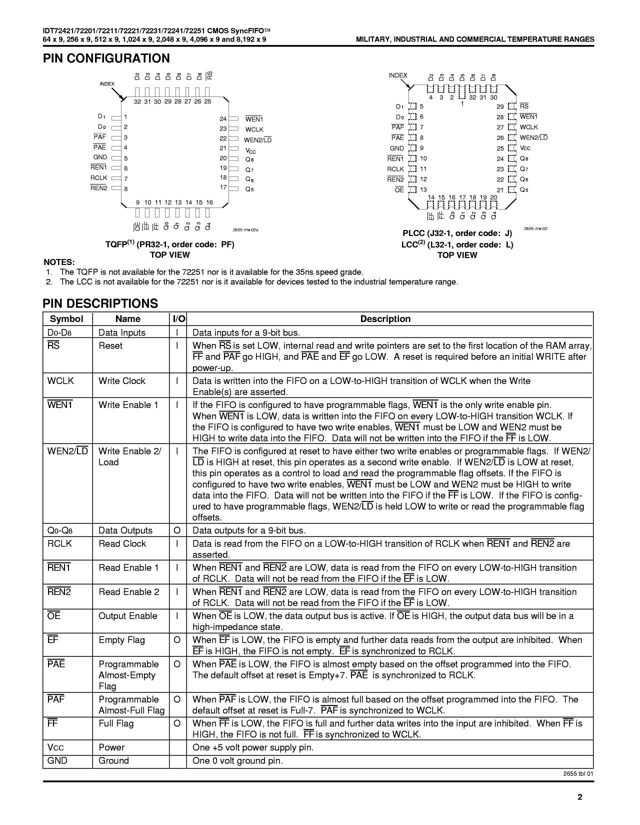
PIN CONFIGURATION
INDEX
D1
D0
PAF
PAE
GND
REN1
RCLK
REN2
32 31 30 29 28 27 26 25
1
24
2
23
3
22
4
PR32-1
21
20
5
19
6
18
7
17
8
9 10 11 12 13 14 15 16
WEN1
WCLK
WEN2/LD
VCC
Q8
Q7
Q6
Q5
MILITARY AND COMMERCIAL TEMPERATURE RANGES
INDEX
D1
D0
PAF
PAE
GND
REN1
RCLK
REN2
OE
4 3 2 32 31 30
5
1
29
6
28
7
27
J32-1
8
L32-1
26
9
25
10
24
11
23
12
22
13
21
14 15 16 17 18 19 20
RS
WEN1
WCLK
WEN2/LD
VCC
Q8
Q7
Q6
Q5
TQFP
TOP VIEW
2655 drw 02a
LCC/PLCC
TOP VIEW
2655 drw 02
PIN DESCRIPTIONS
Symbol
Name
I/O
Description
D0-D8
RS
Data Inputs
Reset
I Data inputs for a 9-bit bus.
I When RS is set LOW, internal read and write pointers are set to the first location of the RAM array,
FF and PAF go HIGH, and PAE and EF go LOW. A reset is required before an initial WRITE after
power-up.
WCLK
Write Clock
I Data is written into the FIFO on a LOW-to-HIGH transition of WCLK when the Write
Enable(s) are asserted.
WEN1
Write Enable 1
I If the FIFO is configured to have programmable flags, WEN1 is the only write enable pin.
When WEN1 is LOW, data is written into the FIFO on every LOW-to-HIGH transition WCLK. If
the FIFO is configured to have two write enables, WEN1 must be LOW and WEN2 must be
HIGH to write data into the FIFO. Data will not be written into the FIFO if the FF is LOW.
WEN2/LD Write Enable 2/ I The FIFO is configured at reset to have either two write enables or programmable flags. If WEN2/
Load
LD is HIGH at reset, this pin operates as a second write enable. If WEN2/LD is LOW at reset,
this pin operates as a control to load and read the programmable flag offsets. If the FIFO is
configured to have two write enables, WEN1 must be LOW and WEN2 must be HIGH to write
data into the FIFO. Data will not be written into the FIFO if the FF is LOW. If the FIFO is config-
ured to have programmable flags, WEN2/LD is held LOW to write or read the programmable flag
offsets.
Q0-Q8
RCLK
REN1
REN2
OE
EF
PAE
PAF
FF
Data Outputs O
Read Clock
I
Read Enable 1 I
Read Enable 2 I
Output Enable I
Empty Flag
O
Programmable O
Almost-Empty
Flag
Programmable O
Almost-Full Flag
Full Flag
O
Data outputs for a 9-bit bus.
Data is read from the FIFO on a LOW-to-HIGH transition of RCLK when REN1 and REN2 are
asserted.
When REN1 and REN2 are LOW, data is read from the FIFO on every LOW-to-HIGH transition
of RCLK. Data will not be read from the FIFO if the EF is LOW.
When REN1 and REN2 are LOW, data is read from the FIFO on every LOW-to-HIGH transition
of RCLK. Data will not be read from the FIFO if the EF is LOW.
When OE is LOW, the data output bus is active. If OE is HIGH, the output data bus will be in a
high-impedance state.
When EF is LOW, the FIFO is empty and further data reads from the output are inhibited. When
EF is HIGH, the FIFO is not empty. EF is synchronized to RCLK.
When PAE is LOW, the FIFO is almost empty based on the offset programmed into the FIFO.
The default offset at reset is Empty+7. PAE is synchronized to RCLK.
When PAF is LOW, the FIFO is almost full based on the offset programmed into the FIFO. The
default offset at reset is Full-7. PAF is synchronized to WCLK.
When FF is LOW, the FIFO is full and further data writes into the input are inhibited. When FF is
HIGH, the FIFO is not full. FF is synchronized to WCLK.
VCC
Power
One +5 volt power supply pin.
GND
Ground
One 0 volt ground pin.
2655 tbl 01
5.07
2
Share Link: