IDT72421L35(1995) データシートの表示(PDF) - Integrated Device Technology
部品番号
コンポーネント説明
メーカー
IDT72421L35
(Rev.:1995)
(Rev.:1995)
Integrated Device Technology

IDT72421L35 Datasheet PDF : 19 Pages
| |||
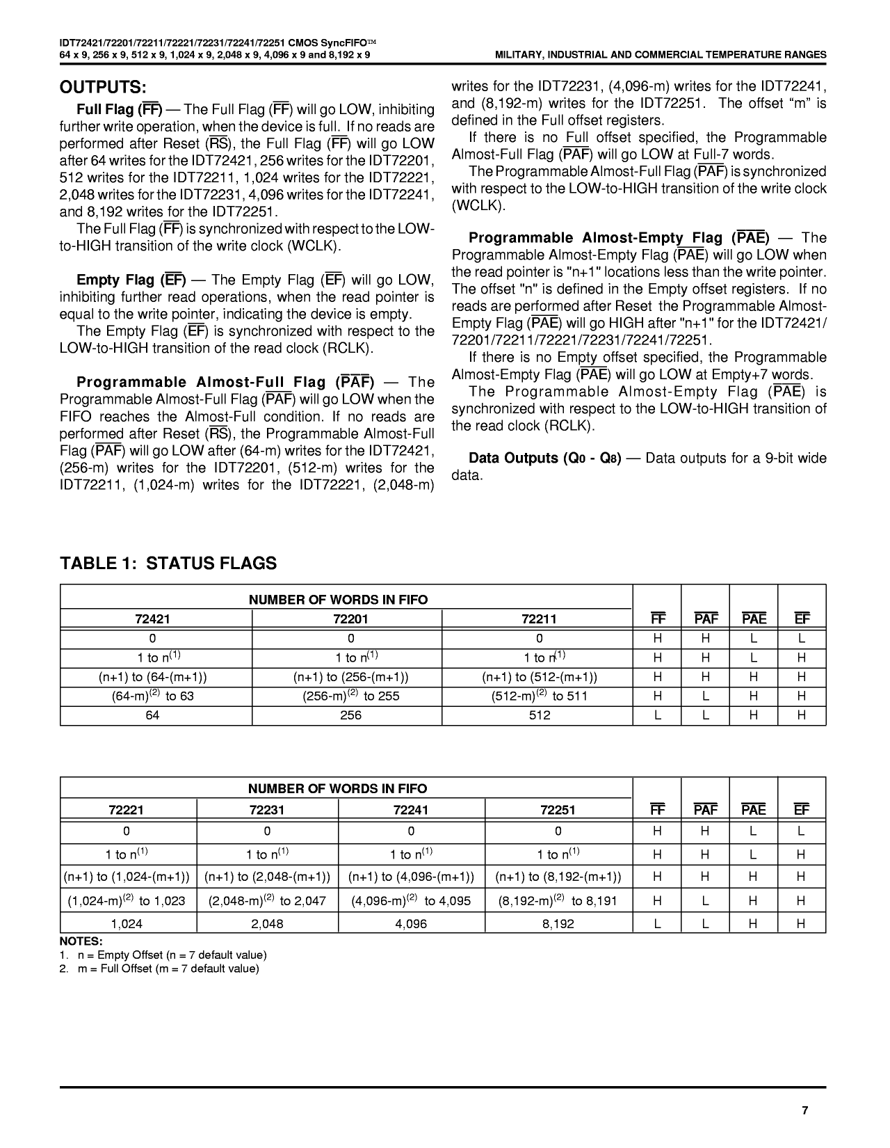
IDT72421/72201/72211/72221/72231/72241 CMOS SyncFIFO™
64 x 9, 256 x 9, 512 x 9, 1024 x 9, 2048 x 9 and 4096 x 9
MILITARY AND COMMERCIAL TEMPERATURE RANGES
However, writing all offset registers does not have to occur
at one time. One or two offset registers can be written and then
by bringing the Write Enable 2/Load (WEN2/LD) pin HIGH, the
FIFO is returned to normal read/write operation. When the
Write Enable 2/Load (WEN2/LD) pin is set LOW, and Write
Enable 1 (WEN1) is LOW, the next offset register in sequence
is written.
The contents of the offset registers can be read on the
output lines when the Write Enable 2/Load (WEN2/LD) pin is
set low and both Read Enables (REN1, REN2) are set LOW.
Data can be read on the LOW-to-HIGH transition of the read
clock (RCLK).
A read and write should not be performed simultaneously
to the offset registers.
LD WEN1 WCLK(1)
Selection
0
0
Empty Offset (LSB)
Empty Offset (MSB)
Full Offset (LSB)
Full Offset (MSB)
0
1
No Operation
1
0
Write Into FIFO
1
1
No Operation
NOTE:
2655 drw 04
1. The same selection sequence applies to reading from the registers. REN1
and REN2 are enabled and read is performed on the LOW-to-HIGH
transition of RCLK.
Figure 2. Write Offset Register
72421 - 64 x 9-BIT
72201 - 256 x 9-BIT
72211 - 512 x 9-BIT
8
65
08 7
08 7
0
Empty Offset (LSB) Reg.
Empty Offset (LSB) Reg.
Empty Offset (LSB)
Default Value 007H
Default Value 007H
Default Value 007H
8
08
08
1
0
(MSB)
0
8
65
08 7
08 7
0
Full Offset (LSB) Reg.
Full Offset (LSB) Reg.
Full Offset (LSB)
Default Value 007H
Default Value 007H
Default Value 007H
8
08
08
1
0
(MSB)
0
72221 - 1024 x 9-BIT
72231 - 2048 x 9-BIT
72241 - 4096 x 9-BIT
8
7
08
7
08
7
0
Empty Offset (LSB) Reg.
Empty Offset (LSB) Reg.
Empty Offset (LSB)
Default Value 007H
Default Value 007H
Default Value 007H
8
1
08
2
08
3
0
(MSB)
(MSB)
(MSB)
00
000
0000
8
7
08
7
08
7
0
Full Offset (LSB) Reg.
Full Offset (LSB) Reg.
Full Offset (LSB)
Default Value 007H
Default Value 007H
Default Value 007H
8
1
08
2
08
3
0
(MSB)
(MSB)
(MSB)
00
000
0000
Figure 3. Offset Register Location and Default Values
2655 drw 05
5.07
7
Share Link: