IDT72421L10(2017) データシートの表示(PDF) - Integrated Device Technology
部品番号
コンポーネント説明
メーカー
IDT72421L10
(Rev.:2017)
(Rev.:2017)
Integrated Device Technology

IDT72421L10 Datasheet PDF : 14 Pages
| |||
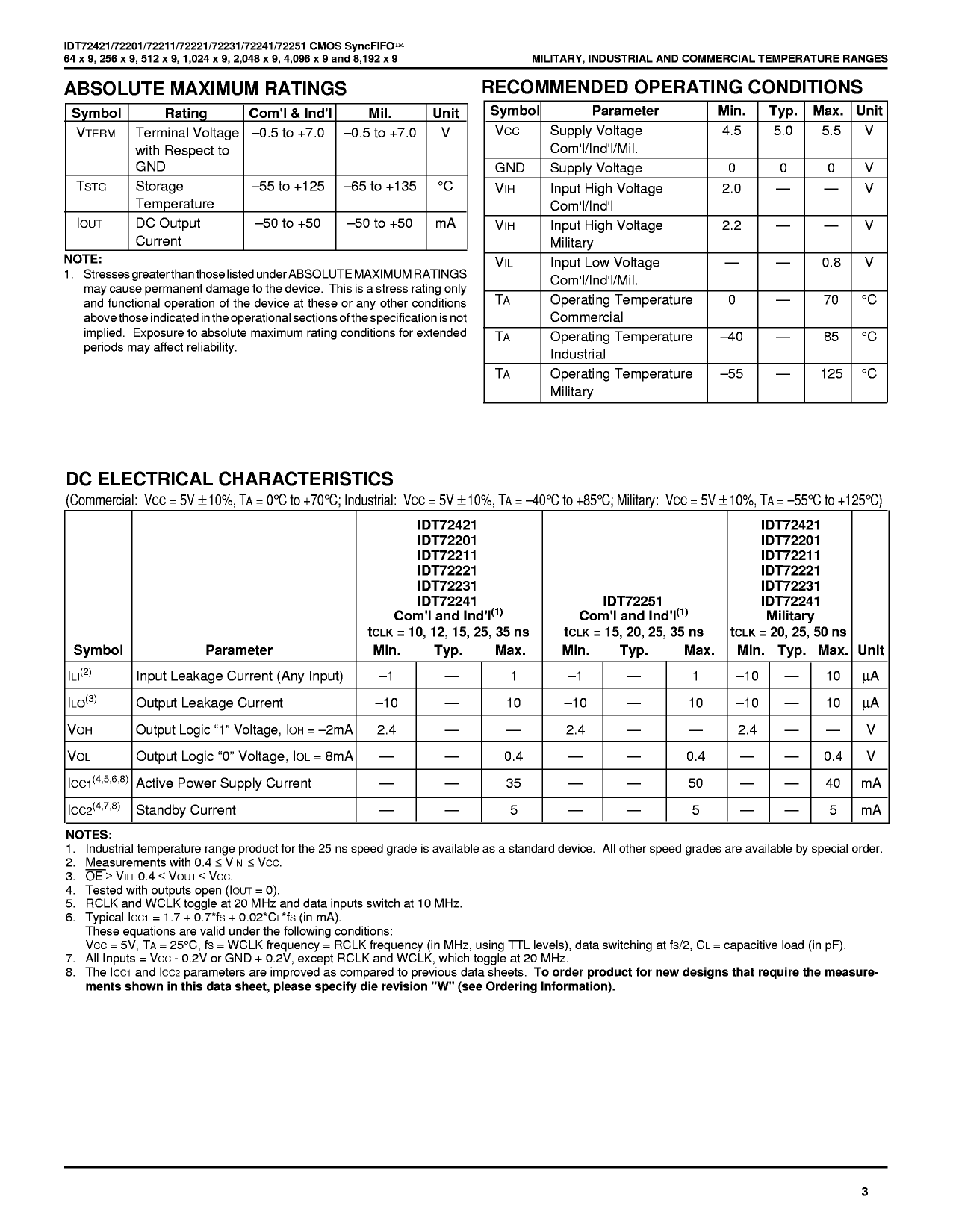
IDT72421/72201/72211/72221/72231/72241/72251 CMOS SyncFIFO™
64 x 9, 256 x 9, 512 x 9, 1,024 x 9, 2,048 x 9, 4,096 x 9 and 8,192 x 9
COMMERCIAL AND INDUSTRIAL
TEMPERATURE RANGES
ABSOLUTE MAXIMUM RATINGS
RECOMMENDED OPERATING
Symbol
Rating
Com'l & Ind'l
Unit
CONDITIONS
VTERM Terminal Voltage with
–0.5 to +7.0
V
Symbol
Parameter
Min. Typ. Max. Unit
Respect to GND
TSTG
Storage Temperature
–55 to +125
°C
IOUT
DC Output Current
–50 to +50
mA
NOTE:
1. Stresses greater than those listed under ABSOLUTE MAXIMUM RATINGS may cause
permanent damage to the device. This is a stress rating only and functional operation
of the device at these or any other conditions above those indicated in the operational
sections of the specification is not implied. Exposure to absolute maximum rating
conditions for extended periods may affect reliability.
VCC
GND
VIH
VIL
TA
TA
Supply Voltage
Commercial/Industrial
Supply Voltage
Input High Voltage
Commercial/Industrial
Input Low Voltage
Commercial/Industrial
Operating Temperature
Commercial
Operating Temperature
Industrial
4.5 5.0 5.5 V
0
00
V
2.0 — — V
— — 0.8 V
0 — +70 °C
–40 — +85 °C
DC ELECTRICAL CHARACTERISTICS
(Commercial: VCC = 5V ± 10%, TA = 0°C to +70°C; Industrial: VCC = 5V ± 10%, TA = –40°C to +85°C)
IDT72421
IDT72201
IDT72211
IDT72221
IDT72231
IDT72241
Com'l and Ind'l(1)
tCLK = 10, 15, 25 ns
IDT72251
Com'l and Ind'l(1)
tCLK = 10, 15, 25 ns
Symbol
Parameter
Min.
Typ.
Max.
Min.
Typ.
Max.
Unit
ILI(2)
Input Leakage Current (Any Input)
–1
—
1
–1
—
1
μA
ILO(3)
Output Leakage Current
–10
—
10
–10
—
10
μA
VOH Output Logic “1” Voltage, IOH = –2mA
2.4
—
—
2.4
—
—
V
VOL
Output Logic “0” Voltage, IOL = 8mA
—
—
0.4
—
—
0.4
V
ICC1(4,5,6)
Active Power Supply Current
—
—
35
—
—
50
mA
ICC2(4,7)
Standby Current
—
—
5
—
—
5
mA
NOTES:
1. Industrial temperature range product for the 15ns and 25ns speed grades are available as standard product.
2. Measurements with 0.4 ≤ VIN ≤ VCC.
3. OE ≥ VIH, 0.4 ≤ VOUT ≤ VCC.
4. Tested with outputs open (IOUT = 0).
5. RCLK and WCLK toggle at 20 MHz and data inputs switch at 10 MHz.
6. Typical ICC1 = 1.7 + 0.7*fS + 0.02*CL*fS (in mA).
These equations are valid under the following conditions:
VCC = 5V, TA = 25°C, fS = WCLK frequency = RCLK frequency (in MHz, using TTL levels), data switching at fS/2, CL = capacitive load (in pF).
7. All Inputs = VCC - 0.2V or GND + 0.2V, except RCLK and WCLK, which toggle at 20 MHz.
©
3
Share Link: