IDT72200 データシートの表示(PDF) - Integrated Device Technology
部品番号
コンポーネント説明
メーカー
IDT72200
Integrated Device Technology

IDT72200 Datasheet PDF : 11 Pages
| |||
IDT72420/72200/72210/72220/72230/72240 CMOS SYNCFIFO™
64 x 8, 256 x 8, 512 x 8, 1,024 x 8, 2,048 x 8, 4,096 x 8
COMMERCIAL TEMPERATURE RANGE
AC ELECTRICAL CHARACTERISTICS
(Commercial: VCC = 5V ± 10%, TA = 0°C to + 70°C)
Symbol
fS
tA
tCLK
tCLKH
tCLKL
tDS
tDH
tENS
tENH
tRS
tRSS
tRSR
tRSF
tOLZ
tOE
tOHZ
tWFF
tREF
tAF
tAE
tSKEW1
tSKEW2
Parameter
Clock Cycle Frequency
Data Access Time
Clock Cycle Time
Clock High Time
Clock Low Time
Data Setup Time
Data Hold Time
Enable Setup Time
Enable Hold Time
Reset Pulse Width(1)
Reset Setup Time
Reset Recovery Time
Reset to Flag and Output Time
Output Enable to Output in Low-Z(2)
Output Enable to Output Valid
Output Enable to Output in High-Z(2)
Write Clock to Full Flag
Read Clock to Empty Flag
Write Clock to Almost-Full Flag
Read Clock to Almost-Empty Flag
Skew time between Read Clock & Write Clock for
Empty Flag & Full Flag
Skew time between Read Clock & Write Clock for
Almost-Empty Flag & Almost-Full Flag
IDT72420L10
IDT72200L10
IDT72210L10
IDT72220L10
IDT72230L10
IDT72240L10
Min.
Max.
—
100
2
6.5
10
—
4.5
—
4.5
—
3
—
0.5
—
3
—
0.5
—
10
—
8
—
8
—
—
10
0
—
2
6
2
6
—
6.5
—
6.5
—
6.5
—
6.5
4
—
10
—
Commercial
IDT72420L15
IDT72200L15
IDT72210L15
IDT72220L15
IDT72230L15
IDT72240L15
Min.
Max.
—
66.7
2
10
15
—
6
—
6
—
4
—
1
—
4
—
1
—
15
—
10
—
10
—
—
15
0
—
3
8
3
8
—
10
—
10
—
10
—
10
6
—
15
—
IDT72420L25
IDT72200L25
IDT72210L25
IDT72220L25
IDT72230L25
IDT72240L25
Min.
Max.
Unit
—
40
MHz
2
15
ns
25
—
ns
10
—
ns
10
—
ns
6
—
ns
1
—
ns
6
—
ns
1
—
ns
15
—
ns
15
—
ns
15
—
ns
—
25
ns
0
—
ns
3
13
ns
3
13
ns
—
15
ns
—
15
ns
—
15
ns
—
15
ns
10
—
ns
18
—
ns
NOTES:
1. Pulse widths less than minimum values are not allowed.
2. Values guaranteed by design, not currently tested.
CAPACITANCE (TA = +25°C, f = 1.0 MHz)
Symbol
Parameter
Conditions Max. Unit
CIN (2)
Input Capacitance
VIN = 0V
10
pF
COUT (1, 2) Output Capacitance
VOUT = 0V
10
pF
NOTES:
1. With output deselected. (OE ≥ VIH)
2. Characterized values, not currently tested.
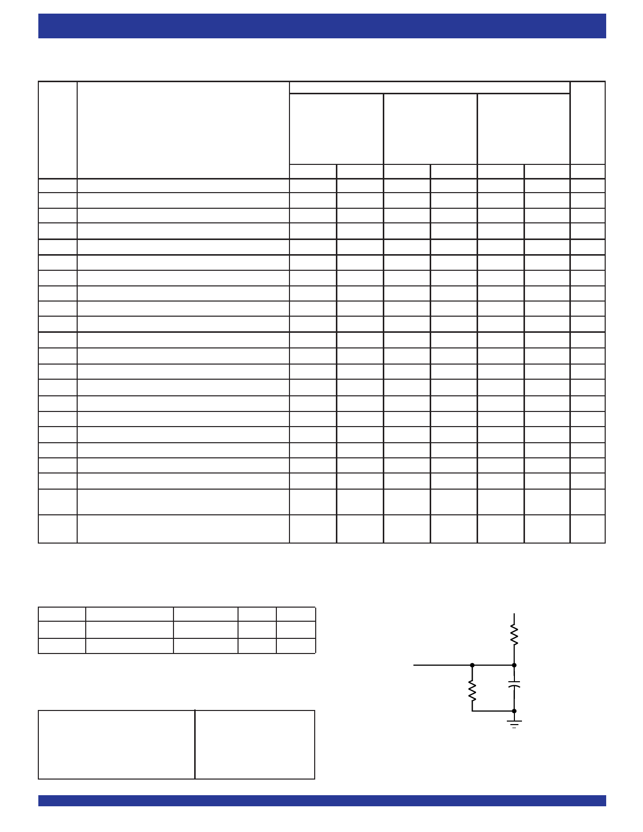
AC TEST CONDITIONS
Input Pulse Levels
Input Rise/Fall Times
Input Timing Reference Levels
Output Reference Levels
Output Load
GND to 3.0V
3ns
1.5V
1.5V
See Figure 1
D.U.T.
680Ω
5V
1.1KΩ
30pF*
2680 drw03
or equivalent circuit
Figure 1. Output Load
*Includes jig and scope capacitances.
4
Share Link: