HV508LG-G(2009) データシートの表示(PDF) - Supertex Inc
部品番号
コンポーネント説明
メーカー
HV508LG-G Datasheet PDF : 4 Pages
| |||
HV508
AC Electrical Characteristics (HVIN = 45V, LVIN = 6.0V, VDD = 5.0V, TA = -5.0°C to +60°C)
Sym Parameter
Min Typ Max Units Conditions
fPOL POL input frequency
0
- 100 Hz ---
tHV(ON)
Turn-on time when high
voltage is enabled
-
-
16
µs Load = 1.0MΩ in parallel with 0.1µF between
tHV(OFF)
Turn-off time when high
voltage is enabled
-
HVOUT1 and HVOUT2, HVEN = high, outputs rise to
-
16
µs HVIN. See Fig.1.
tLV(ON)
Turn-on time when high
voltage is disabled
-
-
40
µs Load = 1.0MΩ in parallel with 0.1µF between
tLV(OFF)
Turn-off time when high
voltage is disabled
-
HVOUT1 and HVOUT2, HVEN = low, outputs rise to
-
6.0
µs HVIN. See Fig.1.
tEN(ON)
Turn-on time from HVEN
to HVOUT
-
-
25
µs
Load = 1.0MΩ in parallel with 0.1µF between
HVOUT1 and HVOUT2. See Fig.2.
Power-Up/ Power-Down Sequences
Power-up sequence should be the following:
1. Connect GND
2. Connect VDD
3. Connect logic inputs
4. Connect HVIN
5. and connect LVIN
Power-down sequence should be the reverse.
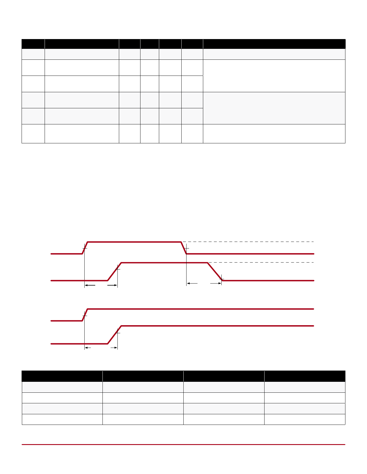
Timing Diagrams
POL
HVOUT1
GND
50%
t(ON)
80%
HVEN
HVOUT1
LVIN
50%
t(ENON)
Logic Truth Table
HVEN
H
H
L
L
80%
POL
H
L
H
L
50%
5%
t(OFF)
Fig. 1
Fig. 2
HVOUT1
HVIN
GND
LVIN
GND
VIH
VIL
HVIN
or LVIN
VIH
VIL
HVIN
HVOUT2
GND
HVIN
GND
LVIN
● 1235 Bordeaux Drive, Sunnyvale, CA 94089 ● Tel: 408-222-8888 ● www.supertex.com
3
Share Link: 