IDTCV193 データシートの表示(PDF) - Integrated Device Technology
部品番号
コンポーネント説明
メーカー
IDTCV193 Datasheet PDF : 21 Pages
| |||
IDTCV193
PROGRAMMABLE FLEXPC CLOCK FOR P4 PROCESSOR
COMMERCIAL TEMPERATURE RANGE
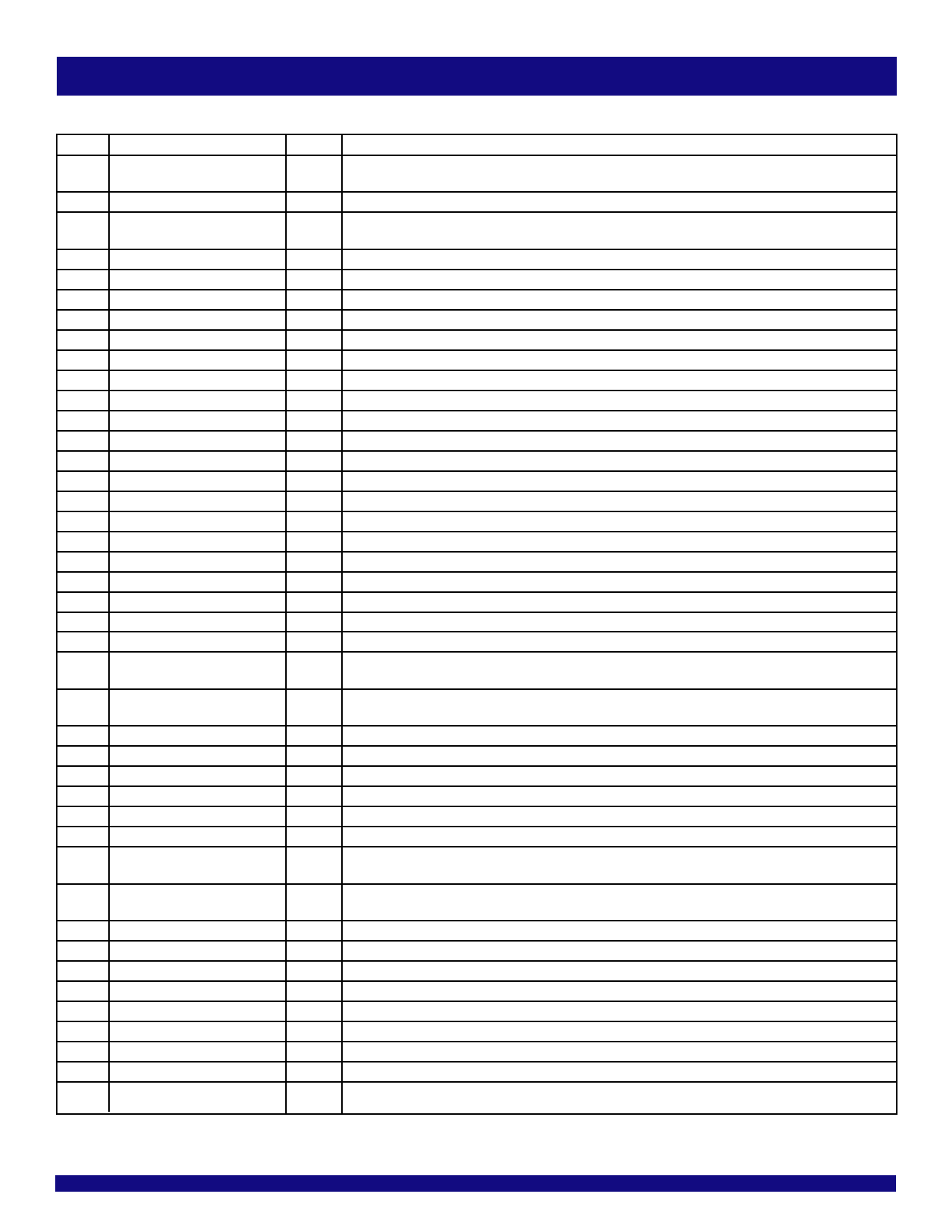
PIN DESCRIPTION
Pin #
Name
Type
1
PCI0/CR#_A
I/O
2
VDD_PCI
PWR
3
PCI1/CR#_B
I/O
4
PCI2/SRC_ENABLE
I/O
5
PCI3/SATA_SEL
OUT
6
PCI4/SRC5_EN
I/O
7
PCIF5/ITP_EN
I/O
8
VSS_PCI
GND
9
VDD_48
PWR
10
USB 48/FS_A
I/O
11
VSS_48
GND
12
VDD_IO
PWR
13
SRCT0/DOT96T
OUT
14
SRCC0/DOT96C
OUT
15
VSS_IO
GND
16
VDD_PLL3
PWR
17
SRCT1/25MHz
OUT
18 SRCC1/25MHz1/24.576MHz OUT
19
VSS_PLL3
GND
20
VDD_PLL3_IO
PWR
21
SATAT/SRCT2
OUT
22
SATAC/SRCC2
OUT
23
VSS_SRC
GND
24
SRCT3/CR#_C
I/O
25
SRCC3/CR#_D
I/O
26
VDD_SRC_IO
PWR
27
SRCT4
OUT
28
SRCC4
OUT
29
VSS_SRC
GND
30
SRCT9
OUT
31
SRCC9
OUT
32
SRCC11/CR#_G
I/O
33
SRCT11/CR#_H
I/O
34
SRCT10
OUT
35
SRCC10
OUT
36
VDD_SRC_IO
PWR
37
CPU_Stop#/SRCC5
I/O
38
PCI_Stop#/SRCT5
I/O
39
VDD_SRC
PWR
40
SRCC6
OUT
41
SRCT6
OUT
42
VSS_SRC
GND
Description
33.33MHz. SRC0, 2 Differential clock output enable, control SRC0 and SRC2, 0 = enable. Mode is selected
by SMBus control register. Default is PCI clock mode.
3.3V
33.33MHz. SRC1, 4 Differential clock output enable, control SRC1 and SRC4, 0 = enable. Mode is selected
by SMBus control register. Default is PCI clock mode.
Power on latch, high, internal 33 ohm resistor enabled. Low, disabled. Afterward 33.33MH
Power on Latch, high, SATA from PLL2. Low, SATA from PLL4 (as SRC clock). Afterward, 33.33MHz
33.33MHz. Pin 37, 38 mode selection. Power on latch, HIGH = SRC5, LOW = CPU and PCI Stop#.
33.33MHz. Pin 46, 47 mode selection. Power on latch, HIGH = CPU_ITP, LOW = SRC8.
GND
3.3V
48MHz, frequency select, power on latch
GND
1.05 ~ 3.3V
Differential output clock. SRC or DOT96. Mode selected by SMBus control register, default is SRC0.
Differential output clock. SRC or DOT96. Mode selected by SMBus control register, default is SRC0.
GND
3.3V
SRC or 25MHz, mode selected by pin 48, Sel_SRC1_25_24.576
SRC or 25Mhz or 24.576MHz, mode selected by pin 48, Sel_SRC1_25_24.576
GND
1.05 ~ 3.3V
Differential output clock
Differential output clock
GND
SRC clock. SRC differential clock output enable, control SRC0 and SRC2, 0 = enable. Mode selected by
SMBus control register. Default is SRC3.
SRC clock. SRC differential clock output enable, control SRC1 and SRC4, 0 = enable. Mode selected by
SMBus control register. Default is SRC3.
1.05 ~ 3.3V
Differential output clock
Differential output clock
GND
Differential output clock
Differential output clock
SRC clock. SRC differential clock output enable, control SRC9, 0 = enable. Mode selected by SMBus control
register. Default is SRC11.
SRC clock. SRC differential clock output enable, control SRC10, 0 = enable. Mode selected by SMBus control
register. Default is SRC11.
Differential output clock
Differential output clock
1.05 ~ 3.3V
CPU stop, LOW = stop. SRC clock. Mode selected by pin6, SRC5_EN.
PCI stop, LOW = stop. SRC clock. Mode selected by pin6, SRC5_EN.
3.3V
Differential output clock
Differential output clock
GND
IDT CONFIDENTIAL
3
Share Link: 