IN24LC02B データシートの表示(PDF) - Integral Corp.
部品番号
コンポーネント説明
メーカー
IN24LC02B Datasheet PDF : 10 Pages
| |||
IN24LC02B
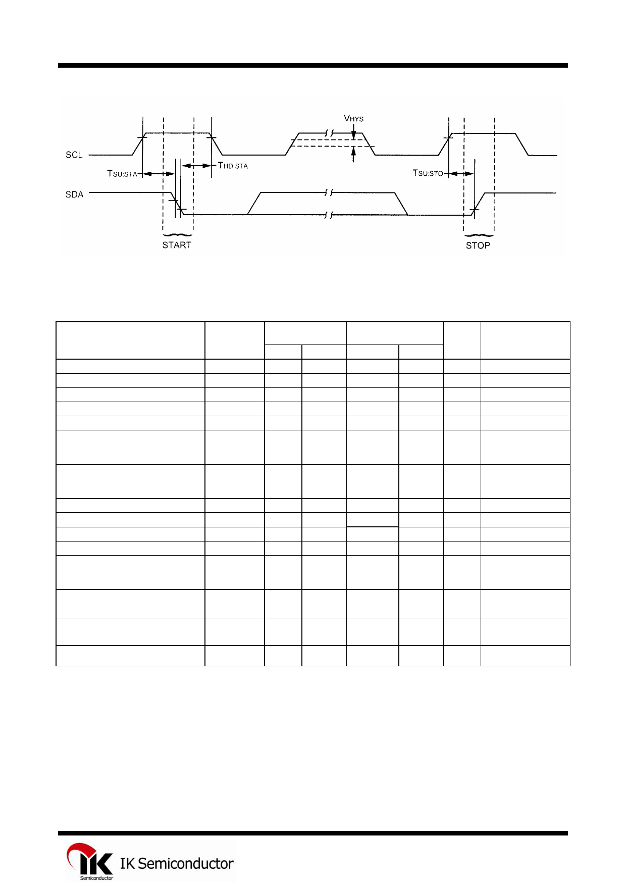
Figure 2. Bus timing Start/Stop
AC CHARACTERISTICS
Parameter
Clock frequency
Clock high time
Clock low time
SDA and SCL rise time
SDA and SCL fall time
START condition hold time
START condition setup time
Data input hold time
Data input setup time
STOP condition setup time
Output valid from clock
Bus free time
Output fall time from VIH min
to VIL max
Input filter spike suppres-sion
(SDA & SCL pins)
Write cycle time
Symbol
FCLK
THIGH
TLOW
TR
TF
THD:STA
TSU:STA
THD:DAT
TSU:DAT
TSU:STO
TAA
TBUF
TOF
TSP
TWR
STANDARD
MODE
Min Max
-
100
4000 -
4700 -
- 1000
-
300
4000 -
4700 -
0
250
4000
-
-
-
-
3500
4700 -
-
250
-
50
-
10
Vcc = 4.5 - 5.5V
FAST MODE
Min Max
-
400
600
-
1300
-
-
300
-
300
600
-
600
-
0
-
100
-
600
-
-
900
1300
-
20+0.1CB 250
-
50
Units Remarks
kHz
ns
ns
ns Note 2
ns Note 2
After this period the
ns first clock pulse is
generated
Only relevant for
ns repeated START
condition
ns
ns
ns
ns Note 1
Time the bus must be
ns free before a new
transmission can start
ns
Note2,
CB≤100pF
ns Note 3
-
10
ms Byte or Page mode
Note 1: As a transmitter, the device must provide an internal minimum delay time to bridge the undefined
region (minimum 300 ns) of the falling edge of SCL to avoid unintended generation of START or
STOP conditions.
Note 2: Not 100% tested. CB = total capacitance of one bus line in pF.
Note 3: The combined TSP and VHYS specifications are due to new Schmitt trigger inputs which provide
improved noise and spike suppression. This eliminates the need for a Ti specification for standard
operation.
3
Share Link: 