IN24LC02B データシートの表示(PDF) - Integral Corp.
部品番号
コンポーネント説明
メーカー
IN24LC02B Datasheet PDF : 10 Pages
| |||
IN24LC02B
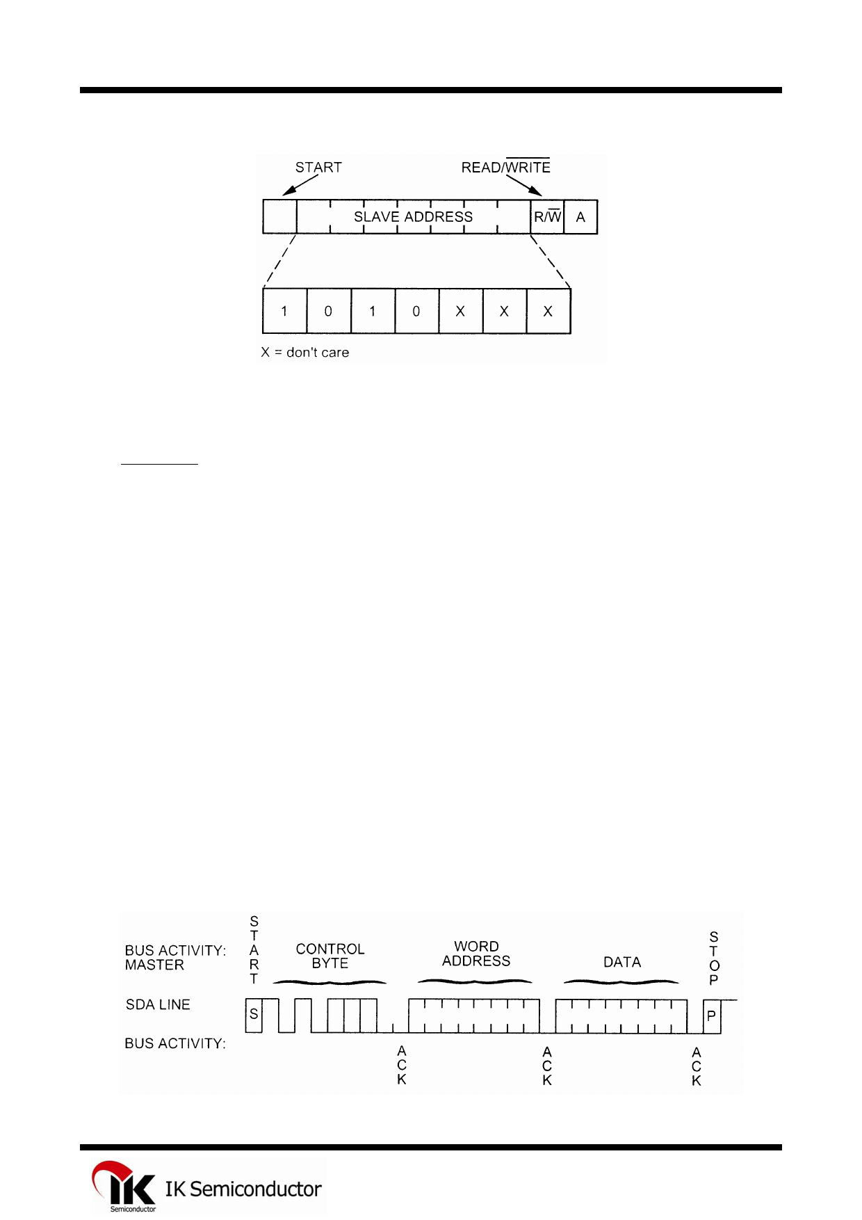
Figure 5. Control Byte Allocation
5.0 WRITE OPERATION
5.1 Byte Write
Following the start condition from the master, the device code (4 bits), the block address (3 bits),
and the R/W bit which is a logic low is placed onto the bus by the master transmitter. This indicates
to the addressed slave receiver that a byte with a word address will follow after it has generated an
acknowledge bit during the ninth clock cycle. Therefore the next byte transmitted by the master is
the word address and will be written into the address pointer of the IN24LC02B. After receiving
another acknowledge signal from the IN24LC02B the master device will transmit the data word to
be written into the addressed memory location. The IN24LC02B acknowledges again and the
master generates a stop condition. This initiates the internal write cycle, and during this time the
IN24LC02B will not generate acknowledge signals (see Figure 6).
Page Write
The write control byte, word address and the first data byte are transmitted to the IN24LC02B in the
same way as in a byte write. But instead of generating a stop condition the master transmits up to
sixteen data bytes to the IN24LC02B which are temporarily stored in the on-chip page buffer and
will be written into the memory after the master has transmitted a stop condition. After the receipt
of each word, the four lower order address pointer bits are internally incremented by one. The
higher order seven bits of the word address remains constant. If the master should transmit more
than sixteen words prior to generating the stop condition, the address counter will roll over and the
previously received data will be overwritten. As with the byte write operation, once the stop
condition is received an internal write cycle will begin (see Figure 8).
Figure 6. Byte Write
6
Share Link: 