IN24LC04N データシートの表示(PDF) - Integral Corp.
部品番号
コンポーネント説明
メーカー
IN24LC04N Datasheet PDF : 10 Pages
| |||
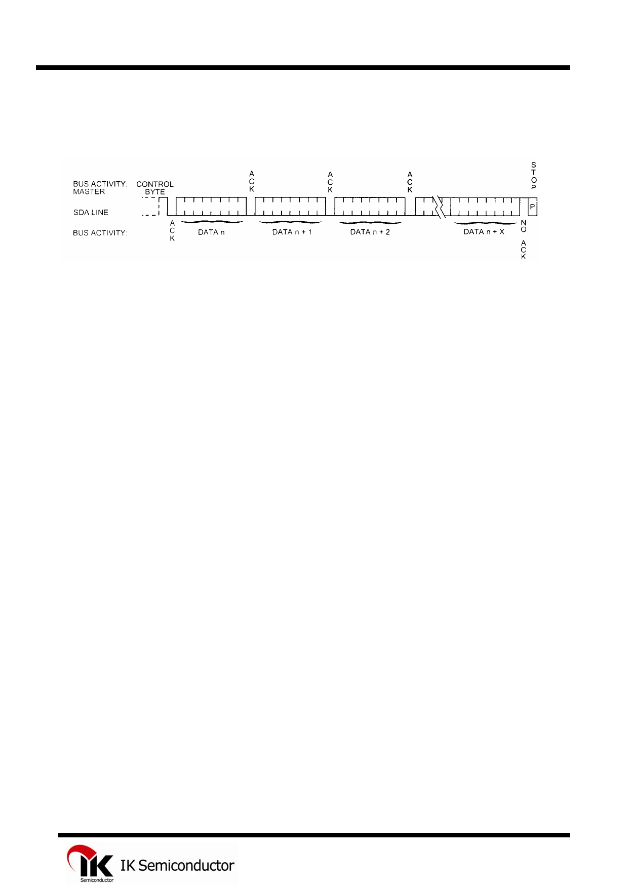
Figure 11. Sequential read
IN24LC04/08
PIN DESCRIPTIONS
SPA Serial Address/Data Input/Output
This is a bidirectional pin used to transfer addresses and data into and data out of the device. It is an
open drain terminal, therefore the SDA bus requires a puliup resistor to Vcc (typical 10KΩ for 100
kHz, 1 KΩ for 400 kHz).
For normal data transfer SDA is allowed to change only during SCL low. Changes during SCL high
are reserved for indicating the START and STOP conditions.
SCL Serial Clock
This input is used to synchronize the data transfer from and to the device.
WP
This pin must be connected to either Vss or Vcc.
If tied to Vss, normal memory operation is enabled (read/write the entire memory).
If tied to Vcc, WRITE operations are inhibited. The entire memory will be write-protected. Read
operations are not affected.
This feature allows the user to use the IN24LC04/08 as a serial ROM when WP is enabled (tied to
Vcc).
A0,A1,A2
These pins are not used by the IN24LC04/08. They may be left floating or tied to either Vss or Vcc.
9
Share Link: 