IN74HC4051A データシートの表示(PDF) - IK Semicon Co., Ltd
部品番号
コンポーネント説明
メーカー
IN74HC4051A Datasheet PDF : 9 Pages
| |||
IN74HC4051A
ADDITIONAL APPLICATION CHARACTERISTICS (GND = 0.0 V)
VCC
Symbol
Parameter
Test Conditions
V
BW Maximum On- fin=1 MHz Sine Wave
Channel
Adjust fin Voltage to Obtain 0 dBm at VOS
Bandwidth or Increase fin Frequence Until dB Meter
2.25
Minimum
Reads -3 dB
4.50
Frequency
RL =50 Ω, CL=10 pF
6.00
Response
(Figure 5)
-
Off-Channel
fin= Sine Wave
Feedthrough
Adjust fin Voltage to Obtain 0 dBm at VIS
Isolation
(Figure 6)
fin = 10 kHz, RL =600 Ω, CL=50 pF
2.25
4.50
6.00
fin = 1.0 MHz, RL =50 Ω, CL=10 pF
2.25
4.50
6.00
-
Feedthrough
VIN≤ 1 Mhz Square Wave (tr = tf = 6 ns)
Noise, Channel Adjust RL at Setup so that IS= 0 A Enable =
Select Input to GND
Common O/I
(Figure 7)
RL =600 Ω, CL=50 pF
2.25
4.50
6.00
RL =10 Ω, CL=10 pF
2.25
4.50
6.00
THD Total Harmonic fin= 1 kHz, RL =10 kΩ, CL=50 pF
Distortion
THD = THDMeasured - THDSource
(Figure 15)
VIS =4.0 VPP sine wave
2.25
VIS =8.0 VPP sine wave
4.50
VIS =11.0 VPP sine wave
6.00
* Limits not tested. Determined by design and verified by qualification.
VEE Limit*
V 25 °C Unit
MHz
-2.25 80
-4.50 80
-6.00 80
dB
-2.25
-4.50
-6.00
-2.25
-4.50
-6.00
-50
-50
-50
-40
-40
-40
mVPP
-2.25 25
-4.50 105
-6.00 135
-2.25 35
-4.50 145
-6.00 190
%
-2.25 0.10
-4.50 0.08
-6.00 0.05
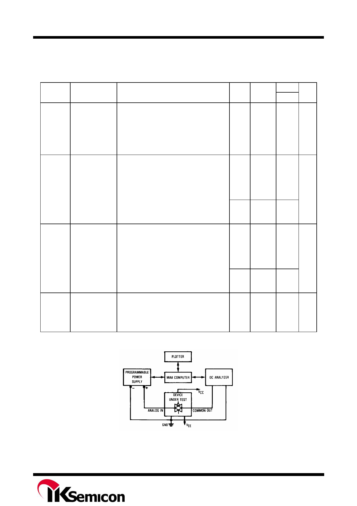
Figure 1. On Resistance Test Set-Up
Rev. 00
Share Link: 