IR2157 データシートの表示(PDF) - International Rectifier
部品番号
コンポーネント説明
メーカー
IR2157 Datasheet PDF : 20 Pages
| |||
ADVANCED INFORMATION
IR2157
Description of Operation & Component Selection Tips
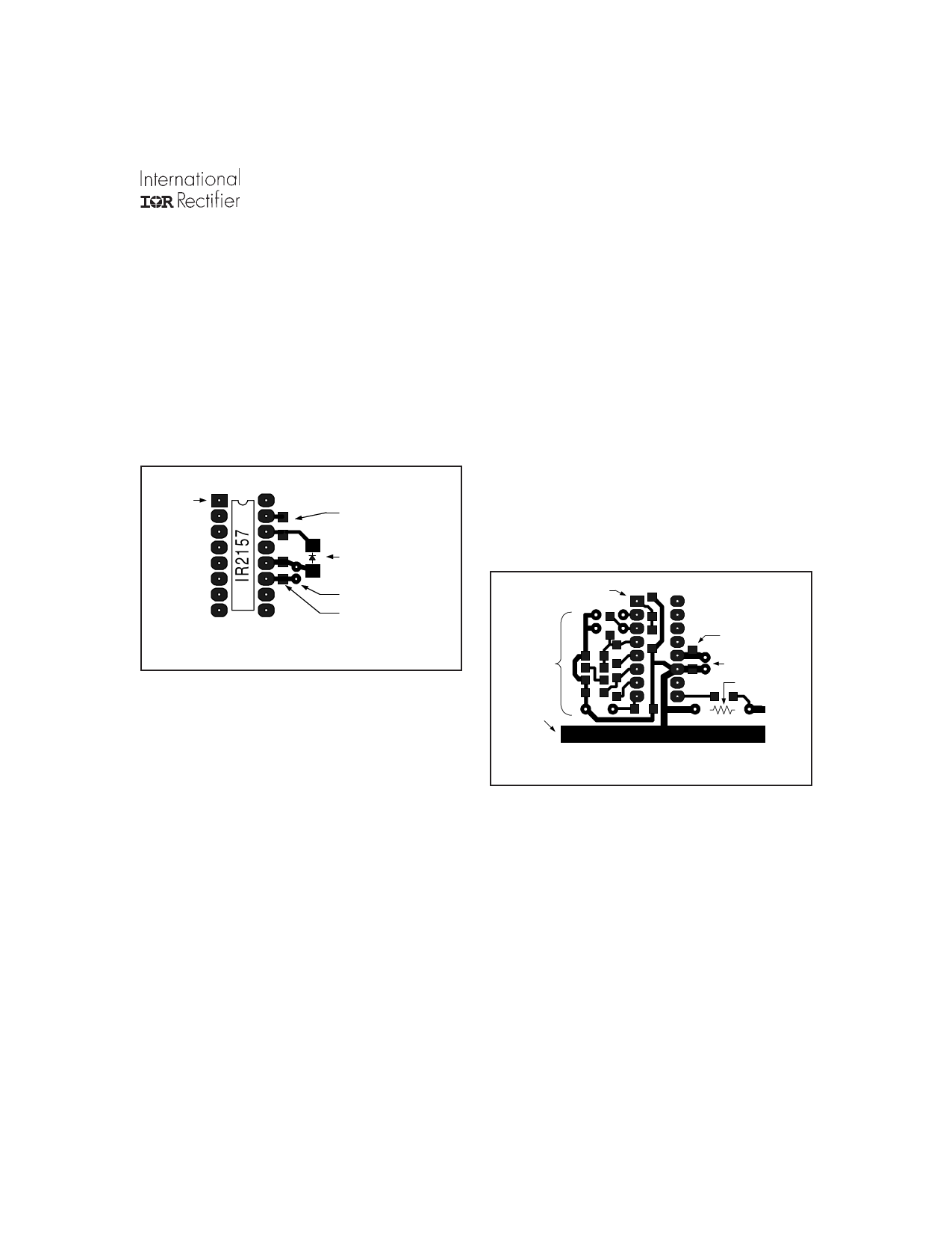
Supply Bypassing and PC Board Layout
Rules
Component selection and placement on the pc
board is extremely important when using power
control ICs VCC should be bypassed to COM as close
to the IC terminals as possible with a low ESR/ESL
capacitor, as shown in Figure 1 below.
pin 1
CBOOT (surface mount)
DBoot (surface mount)
CVCC (through hole)
CVCC (surface mount)
Figure 1: Supply bypassing PCB layout example
A rule of thumb for the value of this bypass capacitor
is to keep its minimum value at least 2500 times the
value of the total input capacitance (Ciss) of the
power transistors being driven. This decoupling
capacitor can be split between a higher valued
electrolytic type and a lower valued ceramic type
connected in parallel, although a good quality
electrolytic (e.g., 10mF) placed immediately adjacent
to the VCC and COM terminals will work well.
In a typical application circuit, the supply voltage to
the IC is normally derived by means of a high value
startup resistor (1/4W) from the rectified line voltage,
in combination with a charge pump from the output
of the half-bridge. With this type of supply
arrangement, the internal 15.6V zener clamp diode
from VCC to COM will determine the steady state IC
supply voltage.
Connecting the IC Ground (COM) to the
Power Ground
Both the low power control circuitry and low side
gate driver output stage grounds return to this pin
within the IC. The COM pin should be connected to
the bottom terminal of the current sense resistor in
the source of the low side power MOSFET using an
individual pc board trace, as shown in Figure 2. In
addition, the ground return path of the timing
components and VCC decoupling capacitor should
be connected directly to the IC COM pin, and not via
separate traces or jumpers to other ground traces on
the board.
IR2157 pin 1
timing
components
VBUS return
CVCC (surface mount)
CVCC (through hole)
RCS (through hole)
Figure 2: COM pin connection PCB layout example
These connection technique prevents high current
ground loops from interfering with sensitive timing
component operation, and allows the entire control
circuit to reject common-mode noise due to output
switching.
9
Share Link: 