ST93C66 データシートの表示(PDF) - STMicroelectronics
部品番号
コンポーネント説明
メーカー
ST93C66 Datasheet PDF : 13 Pages
| |||
ST93C66, ST93C67
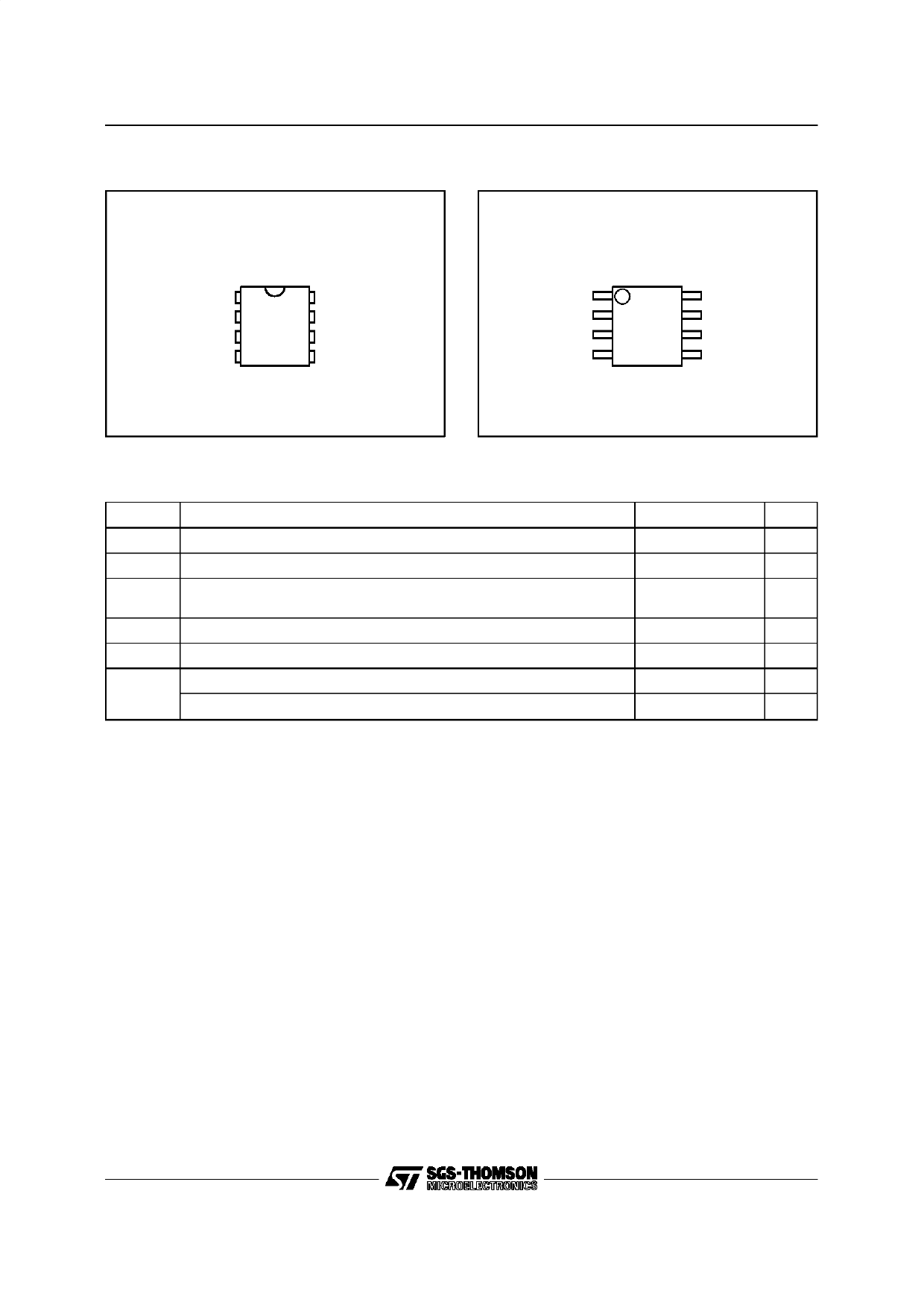
Figure 2A. DIP Pin Connections
Figure 2B. SO Pin Connections
ST93C66
ST93C67
S1
C2
8 VCC
7 DU
D3
6 ORG
Q4
5 VSS
AI01253B
ST93C66
ST93C67
S1
C2
8 VCC
7 DU
D3
6 ORG
Q4
5 VSS
AI01254C
Warning: DU = Don’t Use
Warning: DU = Don’t Use
Table 2. Absolute Maximum Ratings (1)
Symbol
Parameter
Value
Unit
TA
Ambient Operating Temperature
–40 to 125
°C
TSTG Storage Temperature
–65 to 150
°C
TLEAD Lead Temperature, Soldering
(SO8 package)
(PSDIP8 package)
40 sec
10 sec
215
260
°C
VIO
Input or Output Voltages (Q = VOH or Hi-Z)
–0.3 to VCC +0.5
V
VCC
VESD
Supply Voltage
Electrostatic Discharge Voltage (Human Body model) (2)
Electrostatic Discharge Voltage (Machine model) (3)
–0.3 to 6.5
V
7000
V
1000
V
Notes: 1. Except for the rating ”Operating Temperature Range”, stresses above those listed in the Table ”Absolute Maximum Ratings”
may cause permanent damage to the device. These are stress ratings only and operation of the device at these or any other
conditions above those indicated in the Operating sections of this specification is not implied. Exposure to Absolute Maximum
Rating conditions for extended periods may affect device reliability. Refer also to the SGS-THOMSON SURE Program and other
relevant quality documents.
2. MIL-STD-883C, 3015.7 (100pF, 1500 Ω).
3. EIAJ IC-121 (Condition C) (200pF, 0 Ω).
DESCRIPTION (cont’d)
The memory is accessed by a set of instructions
which includes Read a byte/word, Write a
byte/word, Erase a byte/word, Erase All and Write
All. A Read instruction loads the address of the first
byte/word to be read into an internal address
pointer. The data contained at this address is then
clocked out serially. The address pointer is auto-
matically incremented after the data is output and,
if the Chip Select input (S) is held High, the
ST93C66 can output a sequential stream of data
bytes/words. In this way, the memory can be read
as a data stream from 8 to 4096 bits long, or
continuously as the address counter automatically
rolls over to ’00’ when the highest address is
reached. Programming is internally self-timed (the
external clock signal on C input may be discon-
nected or left running after the start of a Write cycle)
and does not require an erase cycle prior to the
Write instruction. The Write instruction writes 8 or
16 bits at one time into one of the 512 bytes or 256
words. After the start of the programming cycle, a
Busy/Ready signal is available on the Data output
(Q) when Chip Select (S) is driven High.
The design of the ST93C66 and the High Endur-
ance CMOS technologyused for its fabrication give
an Erase/Write cycle Endurance of 1,000,000 cy-
cles and a data retention of 40 years.
The DU (Don’t Use) pin does not affect the function
of the memory and it is reserved for use by SGS-
THOMSON during test sequences.The pin may be
left unconnected or may be connected to VCC or
VSS. Direct connection of DU to VSS is recom-
mended for the lowest standby power consump-
tion.
2/13
Share Link: 