ST93C66 データシートの表示(PDF) - STMicroelectronics
部品番号
コンポーネント説明
メーカー
ST93C66 Datasheet PDF : 13 Pages
| |||
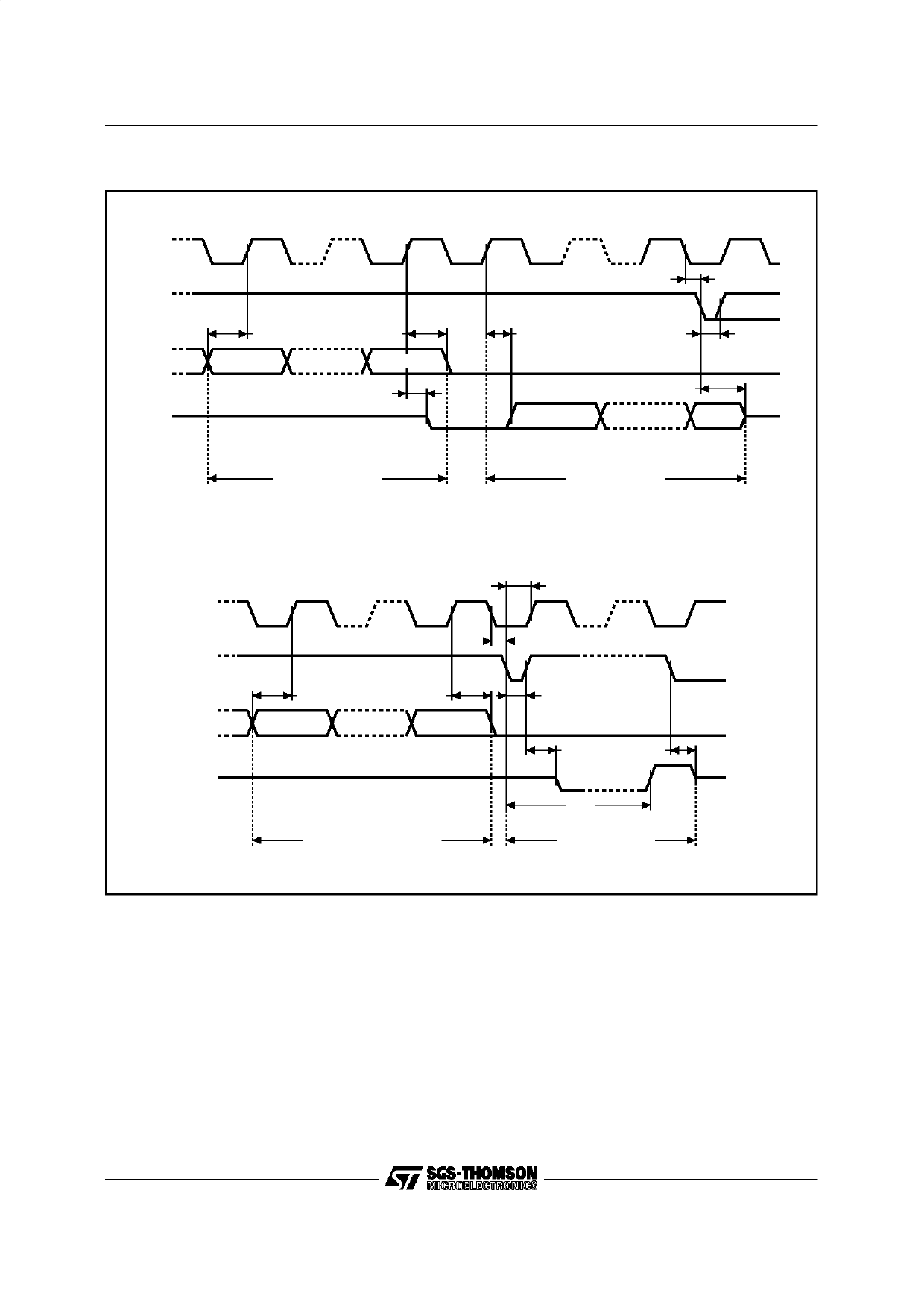
Figure 5. Synchronous Timing, Read or Write
C
S
tDVCH
tCHDX
D
An
A0
Hi-Z
Q
tCHQL
ADDRESS INPUT
ST93C66, ST93C67
tCHQV
Q15/Q7
tCLSL
tSLSH
tSLQZ
Q0
DATA OUTPUT
AI00820C
C
S
tDVCH
D
An
Hi-Z
Q
tCHDX
A0/D0
ADDRESS/DATA INPUT
tSLCH
tCLSL
tSLSH
tSHQV tSLQZ
BUSY
READY
tW
WRITE CYCLE
AI01429
MEMORY ORGANIZATION
The ST93C66 is organized as 512 bytes x 8 bits or
256 words x 16 bits. If the ORG input is left uncon-
nected (or connected to VCC) the x16 organization
is selected, when ORG is connected to Ground
(VSS) the x8 organization is selected. When the
ST93C66 is in standby mode, the ORG input
should be unconnected or set to either VSS or VCC
in order to achieve the minimum power consump-
tion. Any voltage between VSS and VCC applied to
ORG may increase the standby current value.
POWER-ON DATA PROTECTION
In order to prevent data corruption and inadvertent
write operations during power up, a Power On
Reset (POR) circuit resets all internal programming
circuitry and sets the device in the Write Disable
mode. When VCC reaches its functional value, the
device is properly reset (in the Write Disable mode)
and is ready to decode and execute an incoming
instruction. A stable VCC must be applied, before
applying any logic signal.
5/13
Share Link: 