ST93C66 データシートの表示(PDF) - STMicroelectronics
部品番号
コンポーネント説明
メーカー
ST93C66 Datasheet PDF : 13 Pages
| |||
ST93C66, ST93C67
INSTRUCTIONS
The ST93C66 has seven instructions, as shown in
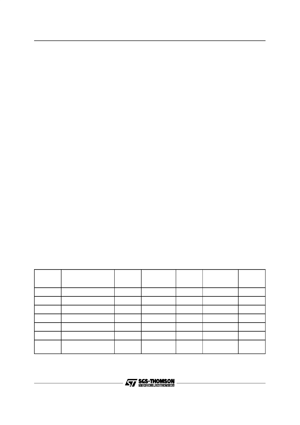
Table 6. The op-codes of the instructions are made
up of 2 bits. The op-code is followed by an address
for the byte/word which is eight bits long for the x16
organization or nine bits long for the x8 organiza-
tion. Each instruction is preceded by the rising edge
of the signal applied on the Chip Select (S) input
(assuming that tha Clock C is low). The data input
D is then sampled upon the following rising edges
of the clock C untill a ’1’ is sampled and decoded
by the ST93C66 as a Start bit.
The ST93C66 is fabricated in CMOS technology
and is therefore able to run from zero Hz (static
input signals) up to the maximum ratings (specified
in Table 5).
Read
The Read instruction (READ) outputs serial data
on the Data Output (Q). When a READ instruction
is received, the instruction and address are de-
coded and the data from the memory is transferred
into an output shift register. A dummy ’0’ bit is output
first, followed by the 8 bit byte or the 16 bit word
with the MSB first. Output data changes are trig-
gered by the Low to High transition of the Clock (C).
The ST93C66 will automatically increment the ad-
dress and will clock out the next byte/word as long
as the Chip Select input (S) is held High. In this
case the dummy ’0’ bit is NOT output between
bytes/words and a continuous stream of data can
be read.
Erase/Write Enable and Disable
The Erase/Write Enable instruction (EWEN)
authorizes the following Erase/Write instructions to
be executed, the Erase/Write Disable instruction
(EWDS) disables the execution of the following
Erase/Write instructions. When power is first ap-
plied, the ST93C66 enters the Disable mode.
When the EWEN instruction is executed, Write
instructions remain enabled until an Erase/Write
Disable instruction (EWDS) is executed or VCC falls
below the power-on reset threshold. To protect the
memory contents from accidental corruption, it is
advisable to issue the EWDS instruction after every
write cycle.
The READ instruction is not affected by the EWEN
or EWDS instructions.
Erase
The Erase instruction (ERASE) programs the ad-
dressed memory byte or word bits to ’1’. Once the
address is correctly decoded, the falling edge of the
Chip Select input (S) triggers a self-timed erase
cycle.
If the ST93C66 is still performing the erase cycle,
the Busy signal (Q = 0) will be returned if S is driven
high, and the ST93C66 will ignore any data on the
bus. When the erase cycle is completed, the Ready
signal (Q = 1) will indicate (if S is driven high) that
the ST93C66 is ready to receive a new instruction.
Write
The Write instruction (WRITE) is followed by the
address and the 8 or 16 data bits to be written. Data
input is sampled on the Low to High transition of
the clock. After the last data bit has been sampled,
Chip Select (S) must be brought Low before the
next rising edge of the clock (C) in order to start
the self-timed programming cycle. If the ST93C66
is still performing the write cycle, the Busy signal
(Q = 0) will be returned if S is driven high, and the
ST93C66 will ignore any data on the bus.
Table 6. Instruction Set
Instruc-
tion
Description
Op-Co de
READ Read Data from Memory
10
WRITE Write Data to Memory
01
EWEN Erase/Write Enable
00
EWDS Erase/Write Disable
00
ERASE Erase Byte or Word
11
ERAL Erase All Memory
00
WRAL
Write All Memory
with same Data
00
Note: 1. X = don’t care bit.
x8 Org
Address
(ORG = 0) (1)
A8-A0
A8-A0
11XXX XXXX
00XXX XXXX
A8-A0
10XXX XXXX
01XXX XXXX
Data
Q7-Q0
D7-D0
D7-D0
x16 Org
Address
(ORG = 1) (1)
A7-A0
A7-A0
11XX XXXX
00XX XXXX
A7-A0
10XX XXXX
01XX XXXX
Data
Q15-Q0
D15-D0
D15-D0
6/13
Share Link: 