IR2238Q データシートの表示(PDF) - International Rectifier
部品番号
コンポーネント説明
メーカー
IR2238Q Datasheet PDF : 17 Pages
| |||
IR2238Q
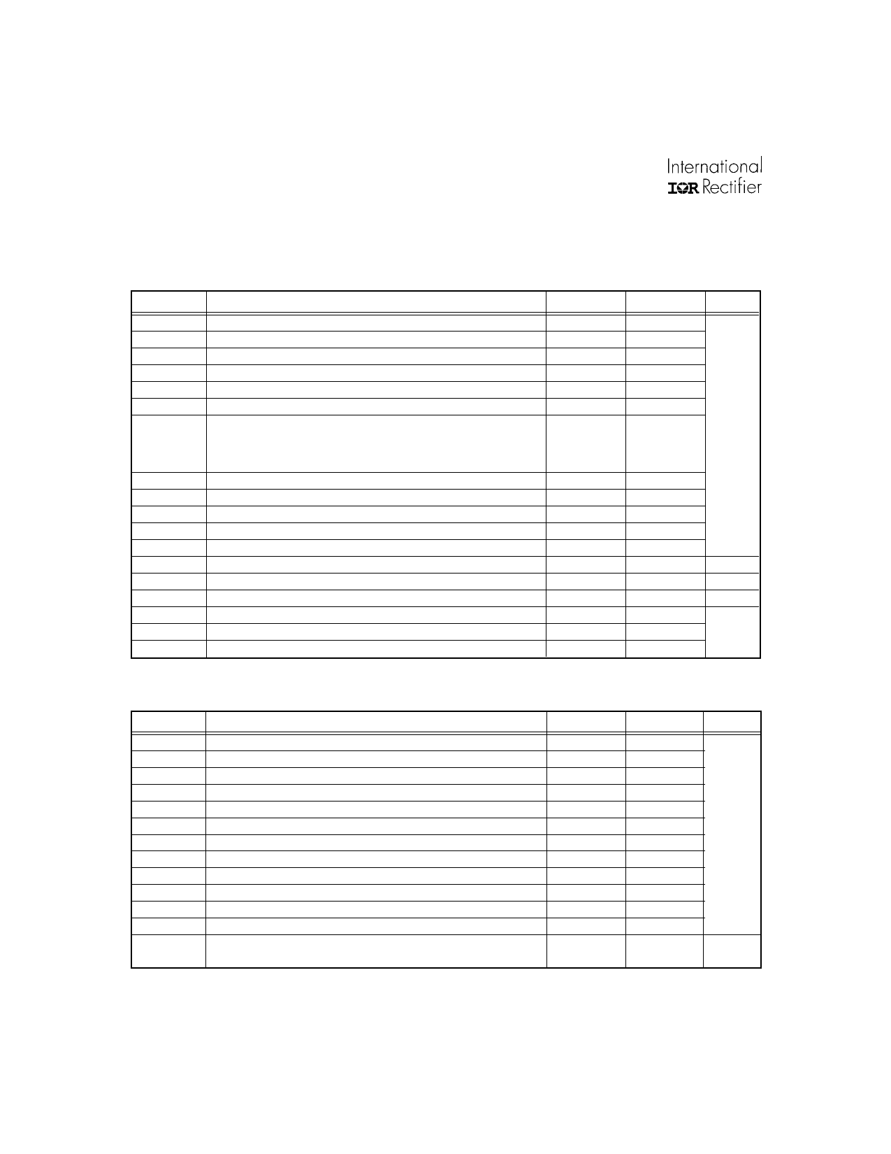
Absolute Maximum Ratings (tentative)
Absolute maximum ratings indicate sustained limits beyond which damage to the device may occur. All voltage parameters
are absolute voltages referenced to COM, all currents are defined positive into any lead. The thermal resistance and power
dissipation ratings are measured under board mounted and still air conditions.
Symbol
Definition
Min.
Max. Units
VS
VB
VHO
VCC
VSS
VLO
VIN
High side offset voltage
High side floating supply voltage
High side floating output voltage (HOP, HON, HOQ)
Low side and logic fixed supply voltage
Logic ground
Low side output voltage (LOP, LON, LOQ)
Logic input voltage (HIN/N,LIN, BRIN/N, SD)
VFLT
VF
VDSH
VDSL
VBR
dVs/dt
PD
RthJA
TJ
TS
TL
FAULT output voltage
Feedback output voltage
High side desat/feedback input voltage
Low side desat/feedback input voltage
Brake output voltage
Allowable offset voltage slew rate
Package power dissipation @ TA ≤ +25°C
Thermal resistance, junction to ambient
Junction temperature
Storage temperature
Lead temperature (soldering, 10 seconds)
VB1,2,3 -25
-0.3
VS1,2,3 - 0.3
-0.3
VCC - 25
-0.3
VSS - 0.3
VSS - 0.3
VSS - 0.3
VS1,2,3 - 0.3
- 0.3
-0.3
—
VB1,2,3 +0.3
1225
VB1,2,3 + 0.3
25
VCC + 0.3
VCC + 0.3
VCC + 0.3 or
VSS + 15
which ever is
lower
VCC + 0.3
VCC + 0.3
VB1,2,3 + 0.3
VCC + 0.3
VCC + 0.3
50
—
2.0
—
60
—
125
-55
150
—
300
V
V/ns
W
°C/W
°C
Recommended Operating Conditions
For proper operation the device should be used within the recommended conditions. All voltage parameters are absolute
voltages referenced to COM. The VS offset rating is tested with all supplies biased at 15V differential.
Symbol
Definition
Min.
Max. Units
VB1,2,3
VS1,2,3
VHO1,2,3
VLO1,2,3
VIN
VCC
VSS
VFLT
VF
VDSH
VDSL
VBR
TA
High side floating supply voltage
High side floating supply offset voltage
High side (HOP/HOQ/HON) output voltage
Low side (LOP/LOQ/LON) output voltage
Logic input voltage (HIN/N,LIN,BRIN/N SD)
Low side supply voltage
Logic ground
FAULT output voltage
Feedback output voltage
High side desat/feedback input voltage
Low side desat/feedback input voltage
BRAKE output voltage
Ambient temperature
VS1,2,3 + 13 VS1,2,3 + 20
Note 1
1200
VS1,2,3
VB1,2,3
VCOM
VCC
VSS
VSS + 5
12.5
20
-5
+5
V
VSS
VSS
VS1,2,3 - 0.3
VCC
VCC
VB1,2,3
- 0.3
VCC
VCOM
-20
VCC
115
°C
Note 1: Logic operational for Vs of COM-5V to COM+1200V. Logic state held for Vs of COM-5V to COM-VBS.
2
www.irf.com
Share Link: 