IS25LD256C データシートの表示(PDF) - Integrated Silicon Solution
部品番号
コンポーネント説明
メーカー
IS25LD256C
Integrated Silicon Solution

IS25LD256C Datasheet PDF : 33 Pages
| |||
IS25LD256C
DEVICE OPERATION
The IS25LD256C utilize an 8-bit instruction register.
Refer to Table 10 Instruction Set for details of the
Instructions and Instruction Codes. All instructions,
addresses, and data are shifted in with the most
significant bit (MSB) first on Serial Data Input (SI). The
input data on SI is latched on the rising edge of Serial
Clock (SCK) after Chip Enable (CE#) is driven low
(VIL). Every instruction sequence starts with a one-byte
instruction code and is followed by address bytes, data
bytes, or both address bytes and data bytes,
depending on the type of instruction. CE# must be
driven high (VIH) after the last bit of the instruction
sequence has been shifted in.
The timing for each instruction is illustrated in the
following operational descriptions.
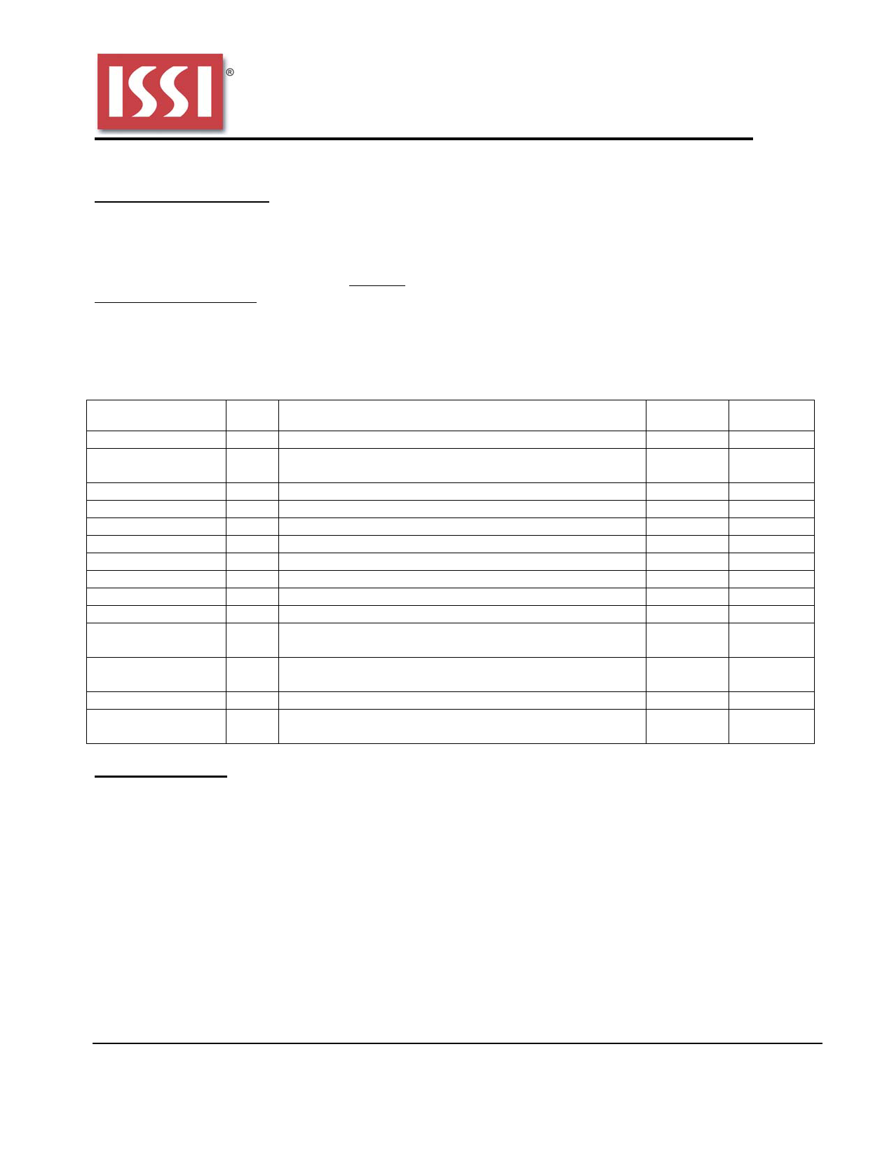
Table 10. Instruction Set
Instruction Name
RDID
JEDEC ID READ
RDMDID
WREN
WRDI
RDSR
WRSR
READ
FAST_READ
FRDO
PAGE_ PROG
SECTOR_ER
BLOCK_ER
CHIP_ER
Hex
Code
ABh
9Fh
90h
06h
04h
05h
01h
03h
0Bh
3Bh
02h
D7h/
20h
D8h
C7h/
60h
Operation
Read Manufacturer and Product ID
Read Manufacturer and Product ID by JEDEC ID
Command
Read Manufacturer and Device ID
Write Enable
Write Disable
Read Status Register
Write Status Register
Read Data Bytes from Memory at Normal Read Mode
Read Data Bytes from Memory at Fast Read Mode
Fast Read Dual Output
Page Program Data Bytes Into Memory
Sector Erase
Block Erase
Chip Erase
Command
Cycle
4 Bytes
1 Byte
4 Bytes
1 Byte
1 Byte
1 Byte
2 Bytes
4 Bytes
5 Bytes
5 Bytes
4 Bytes +
256B
4 Bytes
4 Bytes
1 Byte
Maximum
Frequency
100 MHz
100 MHz
100 MHz
100 MHz
100 MHz
100 MHz
100 MHz
33 MHz
100 MHz
100 MHz
100 MHz
100 MHz
100 MHz
100 MHz
HOLD OPERATION
HOLD# is used in conjunction with CE# to select
the IS25LD256C. When the devices are selected
and a serial sequence is underway, HOLD# can be
used to pause the serial communication with the
master device without resetting the serial sequence.
To pause, HOLD# is brought low while the SCK
signal is low. To resume serial communication,
HOLD# is brought high while the SCK signal is low
(SCK may still toggle during HOLD). Inputs to Sl will
be ignored while SO is in the high impedance state.
Integrated Silicon Solution, Inc.- www.issi.com
10
Rev. A
09/11/2012
Share Link: