IS93C46D データシートの表示(PDF) - Integrated Silicon Solution
部品番号
コンポーネント説明
メーカー
IS93C46D Datasheet PDF : 16 Pages
| |||
IS93C46D
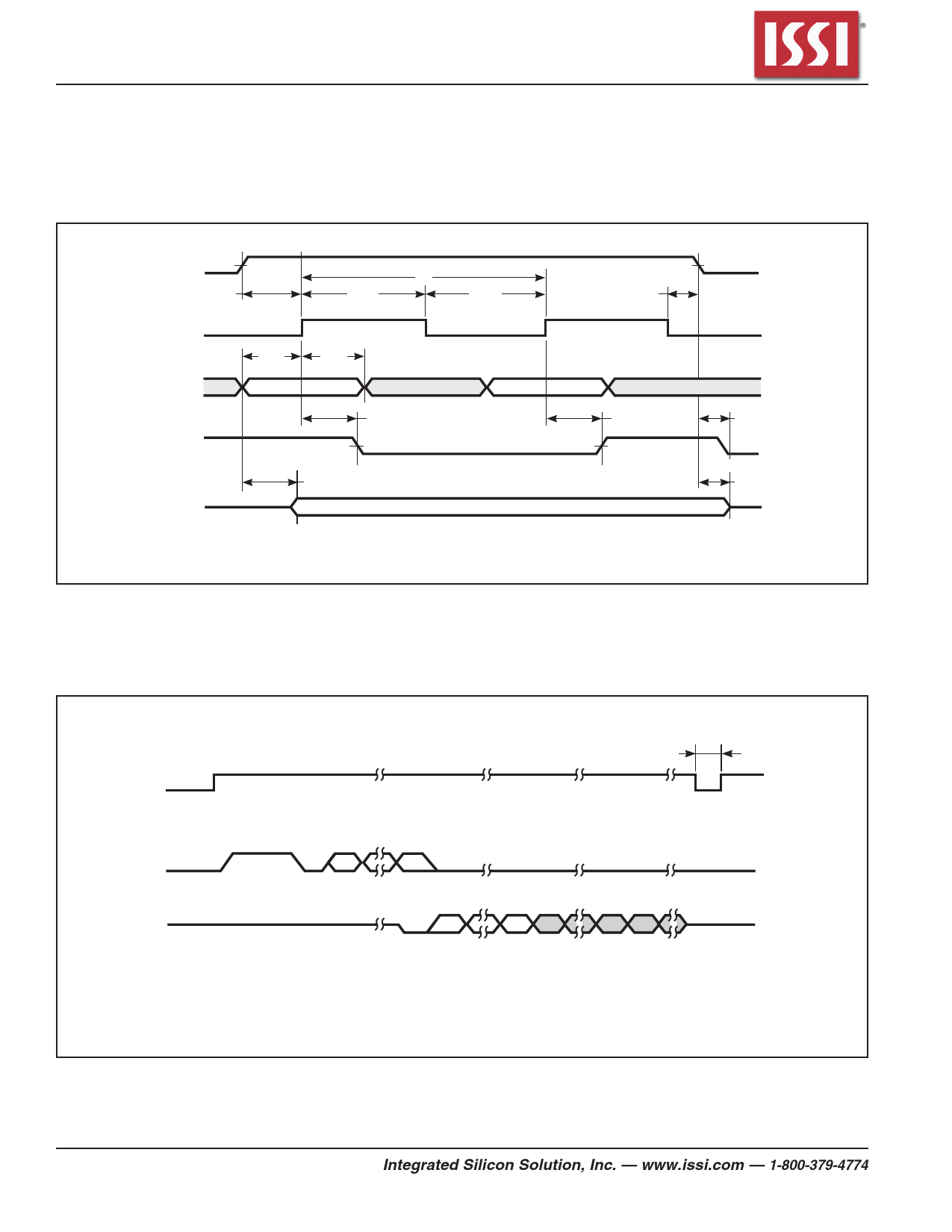
AC WAVEFORMS
FIGURE 2. SYNCHRONOUS DATA TIMING
CS
tCSS
tSKH
T
tSKL
tCSH
SK
DIN
DOUT
(READ)
tDIS
tDIH
tPD0
tPD1
tDF
tSV
tDF
DOUT
(WRITE)
STATUS VALID
(WRALL)
(ERASE)
(ERAL)
FIGURE 3. READ CYCLE TIMING
tCS
CS
DIN
1
1 0 An
A0
DOUT
0 Dm
D0 *
*Address Pointer Cycles to the Next Register
Notes:
To determine address bits An-A0 and data bits Dm-Do, see Instruction Set for the specific device.
8
Integrated Silicon Solution, Inc. — www.issi.com — 1-800-379-4774
Rev. 00G
01/15/07
Share Link: 