IS93C56-3 データシートの表示(PDF) - Integrated Silicon Solution
部品番号
コンポーネント説明
メーカー
IS93C56-3 Datasheet PDF : 10 Pages
| |||
IS93C56-3
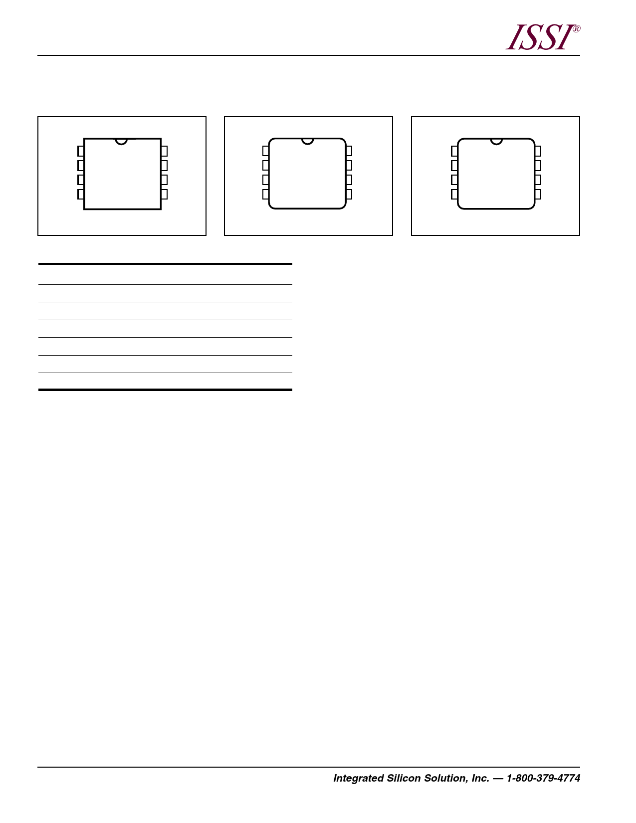
PIN CONFIGURATION
8-Pin DIP
ISSI ®
PIN CONFIGURATION
8-Pin JEDEC Small Outline “G”
PIN CONFIGURATION
8-Pin JEDEC Small Outline “GR”
CS 1
SK 2
DIN 3
DOUT 4
8 VCC
7 NC
6 NC
5 GND
NC 1
VCC 2
CS 3
SK 4
8 NC
7 GND
6 DOUT
5 DIN
CS 1
SK 2
DIN 3
DOUT 4
8 VCC
7 NC
6 NC
5 GND
PIN DESCRIPTIONS
CS
SK
DIN
DOUT
NC
Vcc
GND
Chip Select
Serial Data Clock
Serial Data Input
Serial Data Output
Not Connected
Power
Ground
ENDURANCE AND DATA RETENTION
The IS93C56-3 is designed for applications requiring up to
100,000 programming cycles (WRITE, WRALL, ERASE and
ERAL). It provides 10 years of secure data retention, without
power after the execution of 100,000 programming cycles.
DEVICE OPERATION
The IS93C56-3 is controlled by seven 9-bit instructions.
Instructions are clocked in (serially) on the DIN pin. Each
instruction begins with a logical “1” (the start bit). This is
followed by the opcode (2 bits), the address field (8 bits), and data,
if appropriate. The clock signal (SK) may be halted at any
time and the IS93C56-3 will remain in its last state. This allows
full static flexibility and maximum power conservation.
Read (READ)
The READ instruction is the only instruction that outputs
serial data on the DOUT pin. After the read instruction and
address have been decoded, data is transferred from the
selected memory register into a 16-bit serial shift register.
(Please note that one logical “0” bit precedes the actual
16-bit output data string.) The output on DOUT changes
during the low-to-high transitions of SK (see Figure 3).
Low Voltage Read
The IS93C56-3 has been designed to ensure that data
read operations are reliable in low voltage environments.
The IS93C56-3 is guaranteed to provide accurate data
during read operations with Vcc as low as 2.7V.
Auto Increment Read Operations
In the interest of memory transfer operation applications,
the IS93C56-3 has been designed to output a continuous
stream of memory content in response to a single read
operation instruction. To utilize this function, the system
asserts a read instruction specifying a start location ad-
dress. Once the 16 bits of the addressed word have been
clocked out, the data in consecutively higher address
locations is output. The address will wrap around continu-
ously with CS HIGH until the chip select (CS) control pin is
brought LOW. This allows for single instruction data dumps
to be executed with a minimum of firmware overhead.
Write Enable (WEN)
The write enable (WEN) instruction must be executed
before any device programming (WRITE, WRALL, ERASE,
and ERAL) can be done. When Vcc is applied, this device
2
Integrated Silicon Solution, Inc. — 1-800-379-4774
Rev. G
04/26/01
Share Link: 