55141IRZ データシートの表示(PDF) - Intersil
部品番号
コンポーネント説明
メーカー
55141IRZ Datasheet PDF : 14 Pages
| |||
ISL55141, ISL55142, ISL55143
Absolute Maximum Ratings
VCC to VEE . . . . . . . . . . . . . . . . . . . . . . . . . . . . . . . . . -0.5V to 19V
Input Voltages
PD, CVAX, CVBX, VINPX, VOH, VOL
. . . . . . . . . . . . . . . . . . . . . . . . . . . . . (VEE -0.5V) to (VCC +0.5V)
Output Voltage
QAX, QBX . . . . . . . . . . . . . . . . . . . . . (VOL -0.5V) to (VOH +0.5V)
Thermal Information
Thermal Resistance (Typical, Note 1, 2)
θJA (°C/W)
16 Ld QFN Package. . . . . . . . . . . . . . . . . . . . . . . . .
75
14 Ld TSSOP Package . . . . . . . . . . . . . . . . . . . . . .
90
20 Ld QFN Package. . . . . . . . . . . . . . . . . . . . . . . . .
65
20 Ld TSSOP Package . . . . . . . . . . . . . . . . . . . . . .
80
36 Ld QFN Package. . . . . . . . . . . . . . . . . . . . . . . . .
45
Maximum Junction Temperature (Plastic Package) . . . . . . . 150°C
Maximum Storage Temperature Range . . . . . . . . . . . -65°C to 150°C
Maximum Lead Temperature (Soldering 10s) . . . . . . . . . . . . 300°C
CAUTION: Stresses above those listed in “Absolute Maximum Ratings” may cause permanent damage to the device. This is a stress only rating and operation of the
device at these or any other conditions above those indicated in the operational sections of this specification is not implied.
NOTE:
1. θJA is measured with the component mounted on a high effective thermal conductivity test board in free air. See Tech Brief TB379 for details.
2. Device temperature is closely tied to data-rates, driver loads and overall pin activity. Review Power Dissipation Considerations for more
information.
pO
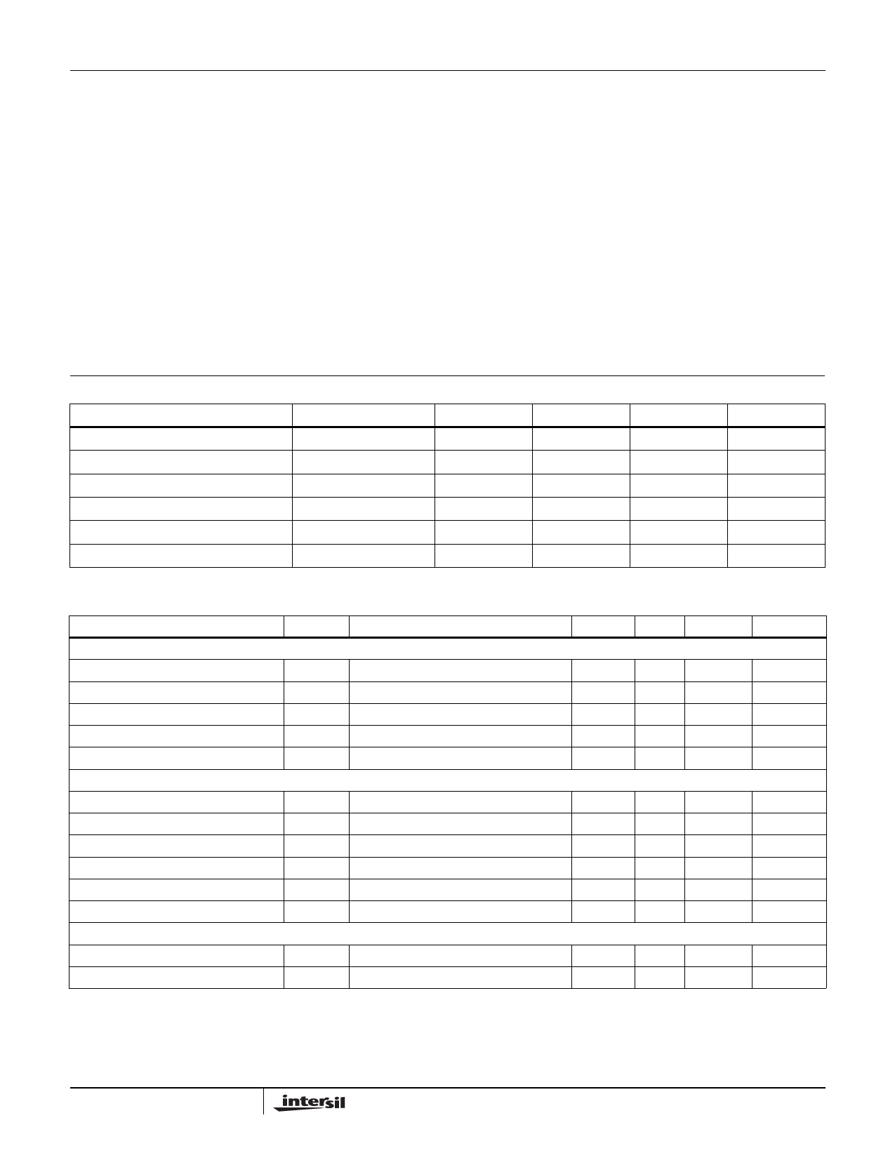
Recommended Operating Conditions
PARAMETER
SYMBOL
Device Power
Comparator Output High Rail
Comparator Output Low Rail
Common Mode Input Voltage Range
Ambient Temperature
Junction Temperature
VCC-VEE
VOH
VOL
VCM
TA
TJ
MIN
10
VEE+1
VEE+0.5
VEE
-40
TYP
15
27
MAX
18
VCC-0.5
VEE+6
VCC-5
+85
+125
UNITS
V
V
V
V
°C
°C
Electrical Specifications
PARAMETER
DC CHARACTERISTICS
Input Offset Voltage
Input Bias Current
Power-down Current
Power-down Time (Note 5)
Power-up Time (Note 5)
TIMING CHARACTERISTICS
Propagation Delay
Rise Time (Note 5)
Fall Time (Note 5)
Propagation Delay Mismatch
Maximum Operating Frequency
Min Pulse Width
COMPARATOR INPUT
Input Current
Input Capacitance (Note 5)
Test Conditions: VCC = 12V, VEE = -3V, VOH = 5V, VOL = 0V, PD = VEE, CLOAD = 15pF, TA = 25°C, unless
otherwise specified.
SYMBOL
TEST CONDITIONS
MIN
TYP
MAX
UNITS
VOS
IBIAS
IPD
tPD
tPU
CVAX = CVBX = 1.5V
VINPX - CV(A/B)X = ±5V
PD = VCC
tpd
tr
tf
Δtpd
FMAXR
tWIDR
Symmetry 50%
IIN
VINPX = VCC or VEE
CIN
-50
50
10
25
8
25
10
15
4.0
9.5
15
1.4
1.5
0.5
2
65
7.7
-100
0
100
2.5
mV
nA
µA
µs
µs
ns
ns
ns
ns
MHz
ns
nA
pF
4
FN6230.0
July 17, 2006
Share Link: 